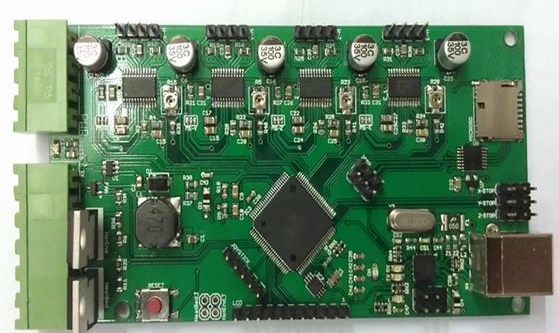
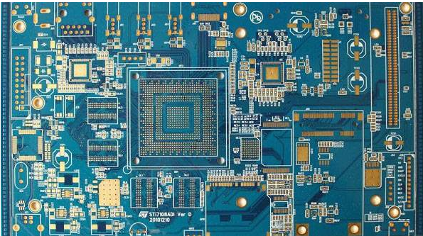
Causes and solutions of PCBA solder joints
At present, the country has higher and higher requirements for environmental protection and greater efforts in link governance. This is a challenge but also an opportunity for PCB factories. If PCB factories are determined to solve the problem of environmental pollution, then FPC flexible circuit board products can be at the forefront of the market, and PCB factories can get opportunities for further development.
1. Judgment of false welding:
1. Use special equipment for online tester (commonly known as needle bed) for inspection.
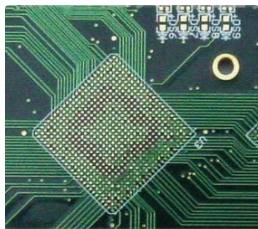
2. Visual inspection (including magnifying glass and microscope). When there is too little solder in the solder joints, poor solder infiltration, or cracks in the middle of the solder joints, or the surface of the solder is convex spherical, or the solder is not compatible with SMD, etc., you should pay attention to it. Even a slight phenomenon will cause If there is a hidden danger, it should be immediately judged whether there is a lot of false welding problem. The method of judgment is: to see if there are many problems with the solder joints at the same position on the PCB. If it is only a problem on a single PCB, it may be caused by the solder paste being scratched, pin deformation, etc., such as the same position on many PCBs. There are problems. At this time, it is likely to be caused by a bad component or a problem with the pad.

2. Causes and solutions of PCBA virtual soldering:
1. The pad design is defective. There should be no through-holes on the pads, as the through-holes will cause solder loss and insufficient solder; the pad spacing and area also need standard matching, otherwise the design should be corrected as soon as possible.
2. The PCB board is oxidized, that is, the pad is black and does not shine. If there is oxidation, an eraser can be used to remove the oxide layer to reproduce the bright light. If the PCB board is damp, it can be dried in a drying box if it is suspected. The PCB board is polluted by oil stains, sweat stains, etc. At this time, it should be cleaned with absolute ethanol.
3. For PCBs that have been printed with solder paste, the solder paste is scratched and rubbed, which reduces the amount of solder paste on the relevant pads and makes the solder insufficient. It should be made up in time. The method of making up can be made up with a dispenser or pick a little with bamboo sticks.
4. SMD (Surface Mount Components) is of poor quality, expired, oxidized, deformed, resulting in virtual soldering. This is a more common reason.
(1) The oxidized components are dark and not shiny. The melting point of the oxide increases. At this time, it can be soldered with more than 300 degrees of electric ferrochrome and rosin-type flux, but with more than 200 degrees of SMT reflow soldering and the use of less corrosive no-clean The solder paste is difficult to melt. Therefore, the oxidized SMD is not suitable for welding with reflow soldering furnace. When buying components, you must see if there is oxidation, and use them in time after you buy them. In the same way, oxidized solder paste cannot be used.
(2) Surface mount components with multiple legs have small legs and are easily deformed under the action of external force. Once deformed, the phenomenon of missing or missing welding will definitely occur. Therefore, it is necessary to carefully check and repair in time before welding.
(3) For PCB s that have been printed with solder paste, the solder paste is scratched and rubbed, which reduces the amount of solder paste on the relevant pads and makes the solder insufficient, which should be made up in time.