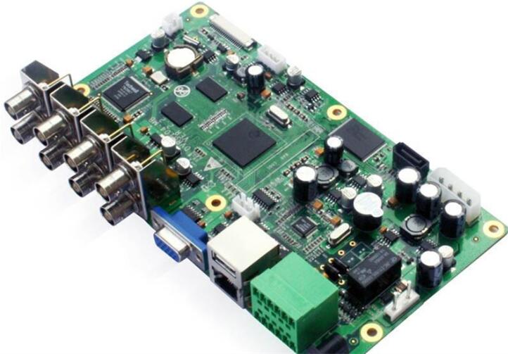
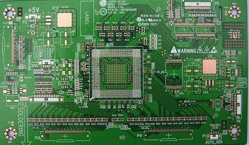
Introduction of components in PCBA
1. Component packaging
Package refers to the layout and structure of component pins. It is the object of assembly and the basis of the design for manufacturability of PCBA processing.
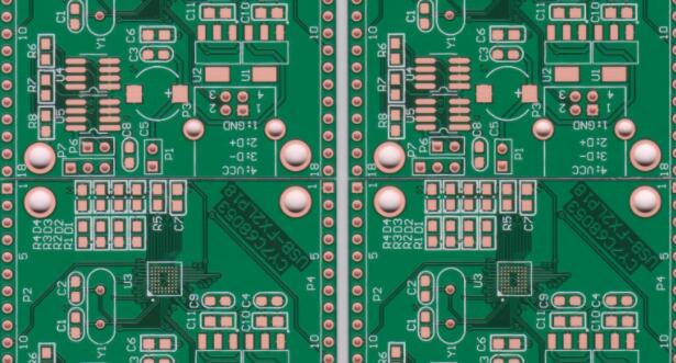
2. Package form of surface mount components
Component layout, pad design, solder mask design and stencil design are all based on the pin structure of the package. Therefore, here we are not classified by the name of the package but by the structure of the pin or solder end. . According to this classification method, the packages of surface mount devices (SMD) mainly include Chip type, J-shaped pin type, L-shaped pin type, BGA type, BTC type, and castle type.
3. Package form of plug-in components
Through Hole Component (THC) packaging, if classified according to the structure type of the lead, there are four main categories, namely, axial lead, radial lead, single in-line and dual-in-line (DIP).

4. Description of acronyms
(1) BGA, the abbreviation of Ball Grid Array, can be translated as a ball grid array package. The solder ends are solder balls and are arranged at the bottom of the package in the form of an array. The ball grid array package includes a full array and a peripheral array. The center distance is L50mm, 1.00mm, 0.80mm, 0.65mm, 0.50mm, 0.40mm and 0.35mm.
(2) BTC, which is the abbreviation of Bottom Termination Component, can be translated as bottom surface end package, and its solder end is flat and laid out on the bottom surface of the package. BTC package includes QFN, LGA, SON, DFN, MLFP, MLP and other package forms.
(3) QFN, the abbreviation of Quad Flat No-Lead Package, can be translated as a quad flat no-lead package, and its solder ends are flat and laid out on the four sides of the bottom of the package.
(4) LGA, which is the abbreviation of LandGridArray, can be translated as land grid array package, and its soldering ends are flat and arranged on the bottom of the package in the form of an array.
(5) SON, the abbreviation of Small Outline No-Lead, can be translated as a small outline no-lead package, and its solder ends are flat and laid out on both sides of the bottom of the package.
(6) MLP, the abbreviation of MicroLeadftamePackage, can be translated as a micro lead frame package, and its solder ends are flat and laid out on the four sides of the bottom of the package. It can be understood as a small-size QFN.
The role of PCBA and measures to prevent damage
Assembly reliability, also known as process reliability, usually refers to the ability of PCBA not to be damaged by normal operations during assembly and soldering. If the design is improper, it is easy to damage or damage the soldered joints or components.
Stress-sensitive devices such as BGA, chip capacitors, and crystal oscillators are easily damaged by mechanical or thermal stress. Therefore, the design should be placed in a place where the PCB is not easily deformed, or reinforced design, or appropriate measures to avoid.
(1) The stress-sensitive components should be placed as far away as possible from the places that are prone to bending during PCB assembly. In order to eliminate the bending deformation during the assembly of the daughter board, the connector that connects the daughter board with the mother board should be placed on the edge of the daughter board as much as possible, and the distance from the screws should not exceed 10mm.
For another example, in order to avoid BGA solder joint stress cracking, it is necessary to avoid placing the BGA layout in a place that is prone to bending during PCB assembly. The poor design of BGA can easily cause its solder joints to crack when holding the board with one hand.
(2) Reinforce the four corners of the large-size BGA.
When the PCB board is bent, the solder joints at the four corners of the BGA are stressed, which is prone to cracks or breaks. Therefore, strengthening the four corners of the BGA is very effective in preventing the cracking of the corner solder joints. Special glue should be used for strengthening, or patch glue can be used for strengthening. This requires space for component layout, and the reinforcement requirements and methods should be indicated on the process documents.
The above two suggestions are mainly considered from the design aspect. On the other hand, the assembly process should be improved to reduce the generation of stress, such as avoiding the use of supporting tools for holding the board with one hand and installing screws. Therefore, the design of assembly reliability should not be limited to the improvement of the layout of the components. The more important thing should be to reduce the stress of the assembly-adopt appropriate methods and tools, strengthen the training of personnel, and standardize the operation actions. Only in this way can the assembly stage be resolved. The problem of solder joint failure.