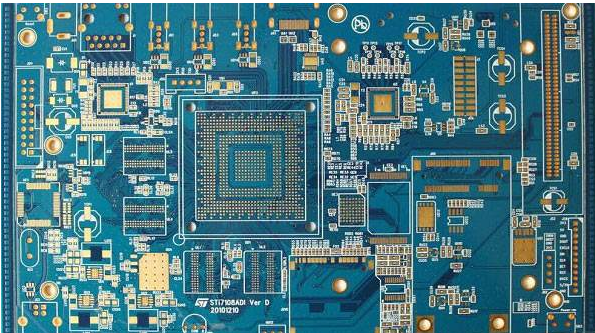
PCBA processing complex technology
Paying attention to the trend of environmental protection informatization and the development of various environmental protection technologies, PCB factories can start with big data to monitor the company's pollution discharge and governance results, and find and solve environmental pollution problems in a timely manner. Keep up with the production concept of the new era, continuously improve resource utilization, and realize green production. Strive to make the PCB factory industry realize an efficient, economical and environmentally friendly production model, and actively respond to the country's environmental protection policy.
As long as we pay attention to the themes of the various professional conferences held in various places today, it is not difficult for us to understand the latest technologies used in electronic products. CSP, 0201 passive components, lead-free soldering, and optoelectronics can be said to be popular advanced technologies that many companies have recently practiced and positively evaluated on PCBs. For example, how to deal with the ultra-small opening (250um) problem that is common in CSP and 0201 assembly is a basic physical problem that has never been encountered before in solder paste printing. Board-level optoelectronic assembly, as a large field developed in communication and network technology, has very fine craftsmanship. Typical packages are expensive and easily damaged, especially after the device leads are formed. The design guidelines of these complex technologies are also very different from ordinary SMT processes, because board design plays a more important role in ensuring assembly productivity and product reliability; for example, for CSP solder interconnection, only through Reliability can be significantly improved by changing the size of the board bonding disk.
CSP application

One of the key technologies that people commonly use today is CSP. The charm of CSP technology lies in its many advantages, such as reduced package size, increased pin count, function/performance enhancement, and package reworkability. The high-efficiency advantage of CSP is embodied in: when used for board-level assembly, it can cross the boundary of fine-pitch (down to 0.075mm) peripheral packaging and enter the larger-pitch (1, 0.8, 0.75, 0.5, 0.4mm) area array structure.
Many CSP devices have been used in consumer telecommunications for many years. It is generally considered that they are low-cost solutions in the fields of SRAM and DRAM, medium pin count ASIC, flash memory and microprocessors. CSP can have four basic characteristic forms: namely rigid base, flexible base, lead frame base and wafer-level scale. CSP technology can replace SOIC and QFP devices and become the mainstream component technology.
One problem with the CSP assembly process is that the bond pads for soldering interconnections are small. Usually the bond pad size of 0.5mm pitch CSP is 0.250~0.275mm. With such a small size, it is difficult to print solder paste through openings with an area ratio of 0.6 or even lower. However, with a well-designed process, printing can be successfully carried out. The failure is usually due to insufficient solder caused by the clogging of the template opening. Board-level reliability mainly depends on the package type, and CSP devices can withstand 800 to 1200 thermal cycles of -40 to 125°C on average without underfilling. However, if underfill materials are used, the thermal reliability of most CSPs can increase by 300%. CSP device failure is generally related to solder fatigue cracking.
Progress in passive components
Another big emerging field is 0201 passive component technology. Due to the market need to reduce the board size, people pay great attention to 0201 components. Since the introduction of 0201 components in mid-1999, cellular phone manufacturers have assembled them with CSPs into phones, reducing the size of the printed board by at least half. Handling this type of package is quite troublesome. To reduce the appearance of post-process defects (such as bridging and erection), the optimization of pad size and component spacing are the key. As long as the design is reasonable, these packages can be placed close to each other, and the spacing can be as small as 150mm.
In addition, 0201 devices can be placed under BGA and larger CSP. Cross-sectional view of 0201 under a 14mm" CSP assembly with 0.8mm pitch. Due to the small size of these small discrete components, assembly equipment manufacturers have planned to develop newer systems compatible with 0201.
Through-hole assembly is still alive
Optoelectronic packaging is being widely used in the telecommunications and network fields where high-speed data transmission is prevalent. Common board-level optoelectronic devices are "butterfly-shaped" modules. The typical leads of these devices extend from the four sides of the package and extend horizontally. The assembling method is the same as that of the through-hole components, usually using a manual process-the lead is processed by a lead forming pressure tool and inserted into the via hole of the printed board to penetrate the substrate.
The main problem with this type of device is the lead damage that may occur during the lead forming process. Since this type of package is very expensive, it must be handled with care to prevent the lead from being damaged by the molding operation or the module package at the lead-device body junction from breaking. In the final analysis, the best solution to integrate optoelectronic components into standard SMT products is to use automatic equipment, so that the components are taken out of the tray, placed on the lead forming tool, and then the leaded device is taken out of the forming machine, and finally Put the module on the printed PCB board. Given that this option requires considerable capital equipment investment, most companies will continue to choose manual assembly processes.
Large-size printed boards (20*24") are also common in many manufacturing fields. Products such as set-top boxes and routing/switch printed boards are quite complex and contain a mixture of the various technologies discussed in this article. For example, in On this type of printed PCB board, large ceramic grid array (CCGA) and BGA devices as large as 40mm2 can often be seen.
The two main problems of this type of device are large-scale heat dissipation and heat-induced warpage effects. These components can act as a large heat sink, causing non-uniform heating under the package surface. Due to the furnace's thermal control and heating curve control, it may lead to non-wetting solder connections near the center of the device. Warpage of the device and printed board caused by heat during processing can cause "non-wetting phenomena" such as separation of the components from the solder paste applied to the printed PCB. Therefore, care must be taken when mapping the heating curves of these printing plates to ensure that the surface of the BGA/CCGA and the entire printing plate are evenly heated.