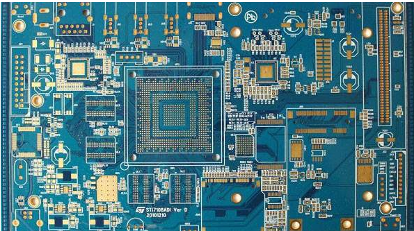
Introduction of Shenzhen PCBA processing solder joint technology essentials
Electronics Co., Ltd. provides one-stop service for Shenzhen PCBA processing, full BOM component purchasing, and PCBA model placement. Mainly based on PCBA sample patch and small and medium batch SMT processing, providing PCBA sample soldering, sample processing, circuit board soldering, BGA soldering, BGA ball planting, BGA packaging processing, BGA flying leads, SMT patch processing, SMT foundry, OEM And other services.
1. The size of solder joints on TOP LAYER and BOTTOM LAYER are the same size
The general SMT process is to solder only one side, so that the solder joints of the plug-in are all on the bottom layer. Key components such as crystal oscillators must be soldered firmly. If the pads are enlarged, attention must be paid at this time: the pads on the top layer should not be too large, otherwise the crystal oscillator may be short-circuited and won't vibrate.
2. Fully use the components in the software component library without any modification
This is what we should in most cases, but sometimes your device may be somewhat different. If you have not used it, confirm whether it matches the components in the library. It is best to measure the actual size to avoid components that cannot be inserted. The catastrophic consequences of pin mismatch.
3. The connection between the PCB and the pad only considers electrical issues, but does not consider REWORK and reliability.
According to the relevant national standards, the PCB board should be left with a maintenance margin of 3-4 times. If this issue is not considered, our wrench may be scrapped once it is removed. Therefore, the mechanical strength, heat dissipation, and adhesion of the part where the pad and the wire are connected must be guaranteed. Generally, we can solve the problem by increasing the area of the pad to strengthen the copper foil as much as possible. In addition, the teardrop-filling function is more meaningful to improve the mechanical strength. (It is better to use arc corners instead of straight corners, including the mechanical layer of the PCB.)
4. Do not indicate the drilling size, only the pad size
Because the pin thickness of the device varies greatly, if the library components are used indiscriminately, the plug-in is not easy or too loose. Excessively large aperture not only causes the components to be loose and tends to sway during wave soldering, but also affects the quality of soldering. There may be insufficient solder joints, half-edge soldering, false soldering, or even not soldering the pins and the pads together.
Regarding the second point, let me add a few words:
1. If the PCB is a single-layer board, do not consider this issue.
2. For PCBs with more than double layers, such as the crystal oscillator (plug-in) mentioned above, it is necessary to consider whether the pad on the component surface will cause a short circuit with the conductive part of the component package. In other words, a short circuit may occur. By analogy, other pad-related phenomena that may cause poor electrical properties should be carefully considered when setting the component pad size.
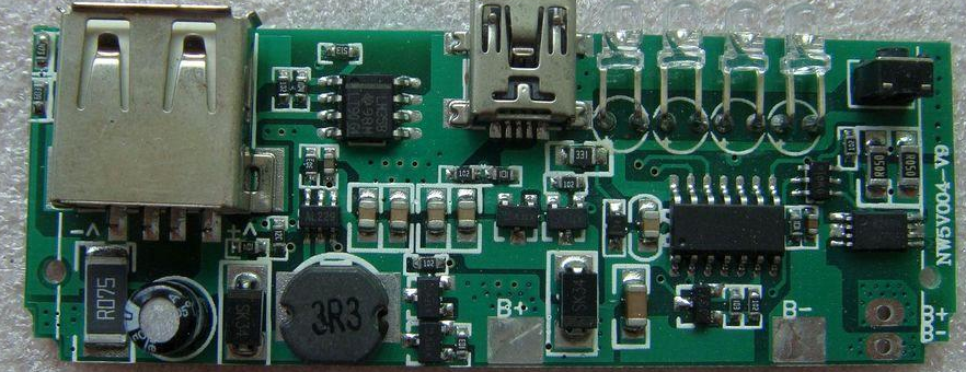
Shenzhen PCBA processing PCB solder joint technology can be divided into DIP and SMT devices, wave soldering and flow soldering welding process. Different devices and processes require different PCB design requirements for solder joints.

The size of the solder joints of DIP devices is determined by the reliability of soldering, and the peel strength of the pads should also be considered for single-sided boards. The size of the aperture is determined by the mechanical structure of the device lead, so that the solder can reach the component surface by using the suction effect during soldering, but there is no solder spatter.
The pads of SMT devices are different from wave soldering and flow soldering and cannot be shared. The component libraries that come with the software are all based on the WAVE process, and the libraries for flow soldering must be self-built. The calculation of the pad is very complicated, but there are empirical formulas that can be applied. There will also be information on the missing screen in the library.
We were established in 2003, committed to providing customers with high-quality PCB electronics manufacturing services for more than 11 years. We proudly declare ourselves as a professional electronic manufacturing service provider. Our confidence comes from the support of more than 5,000 square meters of modern management factory and more than 300 professional employees, and comes from the technical confidence and technical confidence of our strong R&D team. Modern production equipment synchronized with science and technology, more importantly, comes from our scientific management philosophy and excellent execution.