Abstract: PCBA processing companies hope to smoothly import new SMT products to ensure that qualified products are delivered to customers on time. A detailed and comprehensive process review is an indispensable preparation before new product samples. This article starts with PCB DFM design, special components, The main points of the process review are described in detail in three aspects, including the special requirements of customers.
The review content of the SMT foundry contract includes process, quality, price, delivery, service, material loss, packaging and transportation, etc. The most important and key content is the process review, which should include PCB (Printed Circuit Board) ) DFM (Design For Manufacture, design for manufacturability) design, special components, customer's special requirements and other three aspects, respectively, the following detailed descriptions:
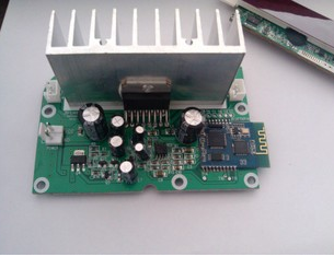
1. DFM design of PCB
The DFM design of PCB is very important. The processability, manufacturability, and testability of PCB can be ensured through DFM design. As an SMT foundry, the main thing that needs to be reviewed is the DFM design content that has a significant impact on the SMT production process.
1. PCB material and temperature resistance
There are many types of PCB materials, and their temperature resistance characteristics are different. Among the commonly used PCB materials, resins include epoxy resin, phenolic resin, etc., and substrates include fiberglass cloth, insulating paper, etc. The more common PCB materials are CEM-1, CEM-3, FR-1, FR-4, FR-5 and other types. The temperature resistance levels of different types of PCB are very different.

For paper PCBs, the temperature resistance level is low and easy to absorb. Due to the characteristics of humidity, it is necessary to set the lowest possible reflow temperature, and at the same time, it is necessary to evaluate whether it is necessary to arrange pre-bake, and pay special attention to non-vacuum-packaged paper PCBs.
2. PCB hollow shape structure
When the hollow area of the irregular-shaped PCB is large, it is easy to cause misdetection of the PCB sensor on the conveyor track of the SMT equipment. It is necessary to increase the detection delay time of the PCB sensor to avoid misoperation due to recognition errors or moving in a direction perpendicular to the track PCB detection sensor to avoid PCB hollowed out.
If it is necessary to arrange the wave soldering process, it is also necessary to consider making a wave soldering carrier board to cover the area with a relatively large hollow, so as to prevent the molten tin from rushing to the board surface.
3. Process side
There can be no components within 4mm of the PCB board edge, otherwise it will affect the SMT production. When it is unavoidable, you can use the method of adding auxiliary edges (process edges) or making the carrier board. The process edges are generally added to the long sides of the PCB, and the width of the process edges is not Less than 3mm, the process side is the same as the PCB flow direction. If PCBA circulation between processes uses a board frame, it is necessary to evaluate whether there are components within the depth of the PCB slot on the board frame (usually 6-7mm).
4. "V-CUT" slot
The PCB board is generally divided by "V-CUT" grooves. The appropriate "V-CUT" groove depth is very important. The "V-CUT" groove can be engraved on both sides or on one side. The total depth is generally the thickness of the PCB. Too shallow will increase the difficulty of splitting the board, too deep will cause insufficient connection strength, and the PCB will be easily deformed when heated by the furnace.
5. PCB thickness
Each SMT device has a limit on the PCB thickness range. Thicker PCBs within the allowable range have good hardness and flatness, and are not easy to deform, so they are more popular with SMT factories, while larger and thinner PCBs are easily deformed. At this time, it is necessary to make a carrier board like a soft board (FPC), and fix the PCB on the carrier board for production.
6. PCB size
Each SMT device has a limit on the PCB size range, too large or too small to produce. If the size of a single-chip PCB is too large, it is necessary to select a large-scale equipment suitable for large-size PCB to produce. If the size of the single-chip PCB is too small, one is to make a multi-board, which makes the PCB size of the multi-board larger; the other is to make a carrier board with a suitable size and place the single-chip PCB on the carrier for production. Of course, the former is produced higher efficiency.
7. PCB pad coating
PCB surface treatment generally includes organic coating (OSP), hot air leveling (tin spraying), electroless nickel/immersion gold (ENIG), immersion silver, immersion tin, etc. The tin spraying board mainly needs to check the flatness of the surface of the solder pad. The unevenness of the spray tin will affect the solder paste printing effect; the OSP board mainly needs to check the oxidation resistance to select the appropriate active solder paste model and the PCB circulation limit time; the PCB surface treated by ENIG is prone to black spots during the soldering process The effect (Black pad) needs to be specially reminded in the PCB appearance inspection SOP (Standard Operating Procedure).
8. PCB solder mask and silk screen
The solder mask cannot cover the pad, and must be able to withstand the high temperature impact of reflow soldering, and it must not produce defects such as peeling and wrinkles. The silk screen characters should be clear and not cover the pads. In particular, pay attention to checking the height of the solder mask and silk screen oil near the fine-pitch IC. Exceeding the standard will increase the thickness of the solder paste on the pin pads of the fine-pitch IC, which may cause poor continuous soldering.
9. Component distribution
The layout of the components should be uniform, neat and compact. The high-power components should be placed in a position that is conducive to heat dissipation. The larger components should be avoided in the center of the board. The thermal components should be far away from the heating components. The same type of plug-in components It should be placed in one direction in the X or Y direction, and the same type of polarized discrete components should be kept consistent in the X or Y direction to facilitate production and inspection. The arrangement of components should be easy to debug and repair, that is, small Large components cannot be placed around the components, and there must be enough space around the components that need to be debugged.
10. Pad and wiring design
1. It is necessary to evaluate whether the pad design matches the actual component. If small components are found to match the large pads, you can consider adding patch glue to the bottom of the component to help fix it, so as to avoid defects such as tombstones and empty soldering during reflow soldering. .
2. It is necessary to evaluate whether the pad size and spacing meet the IPC-SM-782A standard. If it does not meet the requirements, the design needs to be modified, or the minor design defects should be corrected during the design of the printed stencil.
3. There must be no vias on or near the pads of SMD components. The vias are at least 0.5mm away from the pads. Otherwise, during the reflow soldering process, the solder on the pads will flow away along the vias after melting, resulting in empty soldering., Less tin may flow to the other side of the board and cause a short circuit. If it is unavoidable, it is necessary to fill the via hole with glue. If it is a BGA pad, it is also necessary to check that no pits can be left after the via hole is filled, otherwise, the BGA solder joint is prone to voids.
4. The thermal isolation design is required between the pad and the large area copper foil (such as power/ground layer, etc.), otherwise it is easy to cause poor cold welding, and the length of the thermal isolation connection should be at least 1mm.
5. The large-area grounding/power layer should be treated in a grid shape, otherwise, the PCB will be locally deformed due to the large thermal stress difference during the soldering process.
6. If you need to do ICT testing on PCBA, you need to evaluate whether the design of the test pad is reasonable. The two test pads should maintain a distance of 2.54mm or more. The test pads should be tinned. Low-residue no-clean solder paste should be used. Avoid using vias or solder joints instead of test pads.