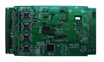
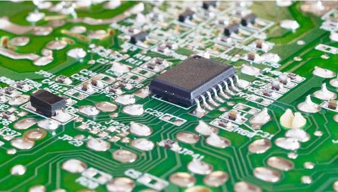
In the process of AIO or QC inspection in SMT chip processing plants, PCBA will more or less show some defective products.
What is the problem, how did it cause it, and what is the state of the bad? So now share it with everyone, as follows:
1. The PCBA circuit board is short-circuited
Refers to the phenomenon of joining between two independent adjacent solder joints after soldering. The cause is that the solder joints are too close, the parts are arranged improperly, the soldering direction is incorrect, the soldering speed is too fast, the flux coating is insufficient, and Poor solderability of parts, poor solder paste coating, excessive solder paste, etc.
2. Empty welding of electronic components
There is no tin on the tin trench, and the parts and the substrate are not welded together. The reasons for this situation are unclean welding trenches, high feet, poor solderability of parts,

extravagant parts, improper dispensing operations, and overflow of glue in the welding trenches. The first class will cause empty welding. The PAD parts of the empty welding are mostly bright and smooth.
3. False welding of electronic components
There is tin between the foot of the part and the welding trench, but it is actually not completely caught by the tin. Most of the reason is that rosin is contained in the solder joints or caused by it.
4. Cold welding of electronic components
Also called undissolved tin, it is caused by insufficient flow soldering temperature or too short flow soldering time. Such a shortcoming can be improved by secondary flow soldering. The surface of the solder paste at cold solder joints is dark and mostly powdery.
5. The electronic components fall off
After the soldering operation, the parts are not in the proper position. The reasons for this are improper selection of glue material or improper glue dispensing operation, incomplete maturation of the glue material, excessive tin wave and too slow soldering speed, etc.
6. Less electronic components
Parts that should be installed but not installed.
7. Damaged electronic components
The appearance of the parts is obviously broken, material defects, or process bumps are caused, or the parts are cracked during the soldering process. Insufficient preheating of parts and substrates, too fast cooling rate after soldering, etc., all contribute to the tendency of parts to crack.
8. Material erosion
This phenomenon mostly occurs on passive parts. It is caused by poor plating treatment on the terminal part of the part. Therefore, when passing through the tin wave, the plating layer melts into the tin bath, causing the structure of the terminal to be damaged, and the solder does not adhere. Good, and higher temperature and longer soldering time will make the bad parts more serious. In addition, the general flow welding temperature is lower than wave welding, but the time is longer. Therefore, if the parts are not good, it will often cause erosion. The solution is to change the parts and control the flow welding temperature and time appropriately. The solder paste with silver content can inhibit the dissolution of the end of the part, and the operation is much more convenient than the change of the solder composition of wave soldering.
9. Solder tip
The surface of the solder joints is not a smooth continuous surface, but has sharp protrusions. The possible causes of this are excessive soldering speed and insufficient flux coating.
10. Less tin on the pad
The amount of tin in the welded parts or parts feet is too small.
11. There are tin balls (beads) on the PCBA board
The amount of tin is spherical, on the PCB, part, or part foot. Poor quality of solder paste or storage for too long, unclean PCB, improper preheating, improper solder paste coating operation, and too long operation time in the steps of solder paste coating, preheating, and flow soldering are all likely to cause solder balls (beads).
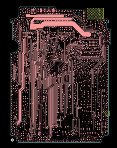
12. PCB open circuit
The line should be turned on but not turned on.
13. Tombstone effect
This phenomenon is also a kind of open circuit, which is easy to occur on CHIP parts. The cause of this phenomenon is that during the soldering process, due to the different tensile forces between the different solder joints of the parts, one end of the part is raised, and the tensile force at both ends is different. So the difference is related to the difference in the amount of solder paste, solderability and tin melting time.
14. Wick effect
This mostly occurs on PLCC parts. The reason for this is that the temperature of the part feet rises higher and faster during flow soldering, or the welding trench is not well wetted, so that after the solder paste melts, it rises along the part feet., Resulting in insufficient solder joints. In addition, insufficient preheating or no preheating, and easier flow of solder paste, etc., will promote this phenomenon.
15. CHIP parts turn white
In the SMT process, the marked surface of the part value is soldered on the PCB upside down, and the part value cannot be seen but the part value is correct, which will not affect the function.
16. Reverse polarity/reverse direction
The component is not placed in the specified orientation.
17. Electronic components shift
18. Too much or not enough glue
19. The electronic components stand side by side
The above is a summary of the problem of defective products after the completion of SMT placement, which has been summarized by a number of SMT placement factories.