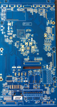
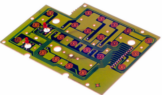
Ten principles for the use of chip inductance during Smt chip processing
1. The spacing of the chip inductors should be smaller than the spacing of the inductors to prevent excessive solder from causing excessive tensile stress to change the inductance value during cooling.
2. The accuracy of the chip inductors that can be purchased on the sales market is mostly ±10%. If the accuracy is required to be higher than ±5%, you need to order in advance.
3. Some chip inductors can be soldered by reflow soldering and wave soldering, but some chip inductors cannot be soldered by wave soldering. When repairing, the inductance cannot be replaced by the inductance alone. It is also necessary to understand the working frequency band of the chip inductors to ensure the working performance.
5. The shape and size of the chip inductors are basically similar, and there is no obvious mark on the shape. When hand soldering or hand patching, don't get the wrong position or take the wrong part.
6. At present, there are three common chip inductors: the first one is high-frequency inductors for microwaves. Suitable for use in frequency bands above 1GHz. The second type is high-frequency chip inductors. It is suitable for resonant circuit and frequency selective circuit. The third type is universal inductance. Generally applicable to circuits of tens of megahertz.

7. Different products have different coil diameters and the same inductance, the DC resistance presented is also different. In the high-frequency circuit, the DC resistance has a great influence on the Q value, so special attention should be paid when designing.
8. The maximum allowable current is also an indicator of chip inductance. When the circuit needs to withstand large currents, this indicator of capacitance must be taken into consideration.
9. When power inductors are used in DC/DC converters, their inductance directly affects the working state of the circuit. In practice, it is often possible to change the inductance by adding or subtracting coils to obtain the best results.
10. For communication equipment operating in the 150~900MHz frequency band, wire-wound inductors are commonly used. In circuits with frequencies above 1GHz, microwave high-frequency inductors must be used.
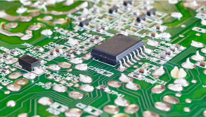
Six common defects and causes in PCBA solder paste printing
In PCBA processing, solder paste printing is a very critical and more complex process. The pros and cons of solder paste printing are not only related to the quality of the solder paste, but also directly related to the equipment and product parameters of the solder paste printing. SMT chip processing manufacturers can improve the printing quality of solder paste by controlling every key point. Next, I will give you a detailed introduction to the six common defects and reasons in solder paste printing.
1. Incomplete printing: Refers to the situation of missing printing on some pads on the PCB.
root cause:
(1) The opening of the steel mesh is blocked or a part of the solder paste is attached to the bottom of the steel mesh;
(2) The viscosity of the solder paste is not up to the standard;
(3) The size of the metal particles in the solder paste is unqualified;
(4) The wear condition of the scraper is serious.
Suggestions for Improvement:
(1) After using the steel mesh, pay attention to the maintenance of the steel mesh and clean it immediately;
(2) Choose solder paste with suitable viscosity;
(3) When selecting solder paste, full consideration should be given to whether the size and particle size of the metal particles are smaller than the size of the openings of the steel mesh;
(4) Regularly inspect and replace the scraper.
2. Sharpening: Refers to the solder paste on the pad with sharp protrusions after the solder paste is printed.
Root cause: There is a problem with the viscosity of the solder paste or the gap of the squeegee is too large.
Suggestions for improvement: select solder paste with suitable viscosity and change the gap of the squeegee.
3. Collapse: It means that the solder paste on the pad collapses to both sides of the pad.
root cause:
(1) The working pressure parameter of the scraper is set too large;
(2) The PCB board is not placed properly, causing an offset;
(3) There is a problem with the viscosity of the solder paste or the metal content is low.
Suggestions for Improvement:
(1) Change the working pressure of the scraper;
(2) Reposition the PCB board;
(3) Re-select the solder paste, taking full account of factors such as viscosity and metal content. Six major solder paste printing defects and analysis in Smt patch processing
4. The solder paste is too thin: the thickness of the solder paste on the pad does not meet the standard.
root cause:
(1) The thickness of the manufactured steel mesh sheet does not meet the standard;
(2) The working pressure product parameter of the scraper is too large;
(3) The solder paste has poor fluidity.
Suggestions for Improvement:
(1) The thickness of the solder paste should be consistent with the thickness of the stencil sheet;
(2) Reduce the working pressure of the scraper;
(3) Choose solder paste with better quality.
5. Different thickness: After printing, the thickness of solder paste is different.
The root cause: the PCB board and the steel mesh are not parallel, and the solder paste is unevenly mixed.
Suggestions for improvement: make PCB and steel mesh as good as possible, and stir evenly before using solder paste.
6. Burrs: There are burrs on the edge or surface of the solder paste
root cause:
(1) The viscosity of the solder paste is too low;
(2) The steel mesh has rough openings.
Suggestions for Improvement:
(1) When determining the solder paste, the viscosity of the solder paste should be fully considered;
(2) Choose the laser method to open holes as much as possible or improve the accuracy of etching.
To improve the solder paste printing quality of smt patch processing, we must start from every key point. From the selection of solder paste, the quality of steel mesh, the product parameters of machinery and equipment, and so on. Every key point will affect the final printing quality.