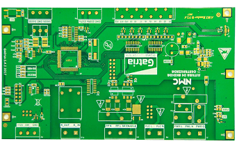
1. Inspection cover
In the SMT production process, when a certain process is completed and ready to enter the next process, there must be a testing process. Because different testing stations have different focus points, different detection covers can be used to shield other parts. Leave only the parts that need to be inspected at this station. The use of the detection cover plate can reduce the labor intensity of the inspector, reduce the rate of false detections and missed detections, thereby greatly improving work efficiency.
2. Microscope
The microscope is a visual inspection tool for inspecting the quality of local welding.
3. Magnifying glass
The magnifying glass is a visual inspection tool for inspecting product quality.
4. Digital camera
Digital cameras can record visual records such as quality and defects in the production process of products.

5. Thrust gauge
Thrust gauge is an instrument for testing the welding strength of components after welding.
SMT patch processing 011
6. Needle bed fixture
The needle bed fixture is a fixture to be installed on the inspection equipment when the online needle bed tester is used to perform static and dynamic inspections of the product after the product is produced. It cooperates with the inspection software to inspect the product.
1) Needle bed manufacturing
Needle bed devices are usually fixed, compact or fastened structures. There are generally 4 types of needle bed clamps, namely, open type, cylinder type, mechanical cylinder hybrid type and work bench. Generally, the position coordinates of the test probes of the through-hole circuit board can be read from the bare board or the wiring film with a digital instrument. For high-density circuit boards, the needle bed should be made using the PCB design software data to ensure the positioning accuracy of the probe points . Usually, the standard materials required for production include probe serial number data, mounted circuit board schematic diagram and component table.
2) Selection of probe shape
Regardless of the online test equipment, in terms of its technical structure characteristics, the test probe is its core and key component. It is divided into two types of structures. One is a spring-buffered type, which relies on a specific needle bed or auxiliary device to apply pressure to ensure close and reliable contact between the probe and the measured point. This type of probe is the most common; the other is a pneumatic probe, which is The high-pressure airflow drives the needle head to achieve close contact with the measured point. The probe is mainly used to connect the test signal to the test point of the circuit board under test. From a simple bare board test to a relatively single pointed probe, after years of technical research and development, it has developed into a more systematic series of standard products. Each type of probe has its corresponding test object and specific requirements. In actual production, it should be selected according to its manufacturer's recommendations and actual production conditions.
3) Selection of probe contact point
The probe contacts of surface mount circuit boards usually include test pads, trace vias, and pins. The selection of probe contacts can be carried out in the following order: specially designed test pads, chip pads above 2125, IC pin pads with a pitch of 0.8 mm or more, vias (when there are components), bare holes ( There should be no solder mask), chip pads below 1608 (designated 2 points), etc. Attention should be paid to the newly designed printed circuit board wiring: the area of the test pad is above 0.4 mmx0.4 mm; the minimum spacing of the probes is above 1.27 mm; the components should not cover the probe contacts.
4) PCB inspection positioning mark
The positioning mark for PCB inspection can borrow the optical identification mark on the placement machine. If not, use the point coordinates of the test probe generated from the CAD data. With the help of wiring fiducial marks on the printed circuit board, positioning marks for PCB testing are added, which can reduce the manufacturing error of the tested printed circuit board and the setting error of the printed circuit board, thereby realizing high-precision measurement. Commonly used fiducial marks are ■, ▲, • and so on. Due to the high manufacturing cost, complex structure, and easy damage of the needle bed, all the needles on the needle bed must be in close contact with the test point, and the pressure on each needle must be uniform. Therefore, the force must be uniform during use, and the probe must be frequently tested. The needle contact function is checked to ensure that the needle bed is in good working condition.