Abstract and complex digital high-speed logic principles, and how to transmit square wave signals in the transmission line, and how to ensure its signal integrity (Signal Integrity), reduce its noise (Noise) to reduce the misoperation and other professional expressions, if you can use simple Life examples are used to illustrate, but if you bring in a bunch of mathematical formulas and difficult physical languages instead of moving, the enlightenment and blessings of novices or interveners will be more effective if less effort is needed.
However, many undergraduate professionals, even doctors and professors whose teachers are in Xingtan, don't know if they have not yet really entered the situation and do not know why? Or they deliberately show off what they know in order to frighten the educated, but they don’t know, or they have both mentalities! There are a large number of books and journal articles in the market, and most of them are inexplicable. There are few examples. It really makes people look at the flowers in the fog. It is strange to understand it!
The author recently obtained a briefing information about impedance control, which was provided by Nissho HIOKI, a professional electrical testing company. The content can be said to be comprehensible at a glance, which makes people love it. It is the realm that the author has been pursuing for a long time. I am overjoyed with the consent of the original "Wen Kong Construction" company, with the strong assistance of Hong Kong Construction Company Vice President Liao Fengying, as well as the original author Hiroshi Yamazaki and his superiors. Thanks to Toshihiko Kanai and others for being able to complete this article. And welcome all seniors and advanced students to give a lot of similar information to benefit the student readers, and you will be very good in the industry.
1. Treat the signal transmission as a hose for watering flowers
1.1 In the multi-layer board signal line of the digital system, when the square wave signal is transmitted, it can be imagined as a hose to send water to the flowers. One end is pressurized in the hand grip to make it shoot out the water column, and the other end is connected to the faucet. When the pressure exerted by the grip tube is just right, and the range of the water column is correctly sprayed on the target area, both the giving and receiving will be happy and the mission will be successfully completed. Isn't it a handy little achievement?
1.2 However, once the water injection process is too far, it will not only vacate the target and waste water resources, but may even have nowhere to vent due to the strong water pressure, so that it may rebound from the source and cause the hose to break free from the faucet! Not only the mission failed, it was also a big frustration. It's so prickly and full of bean curd!
1.3 On the contrary, when the grip is not squeezed enough to make the range too close, the desired result will still not be obtained. Too much is not what you want. Only when it is just right can everyone be happy.
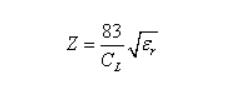
1.4 The above simple details of life can be used to illustrate that square wave (Square Wave) signals (Signal) are carried out in multi-layer board transmission lines (Transmission Line, which is composed of signal lines, dielectric layers, and ground layers). Fast delivery. At this time, the transmission line (commonly known as Coaxial Cable, Microstrip Line or Strip Line, etc.) can be regarded as a hose, and the pressure applied by the holding tube is like the "receiving end" on the board. (Receiver) The resistor connected in parallel to Gnd is general (it is one of the five terminal technologies, please refer to the article "Development of Embedded Resistors" in the 13th issue of TPCA Proceedings for detailed description), which can be used to adjust its end point Characteristic Impedance (Characteristic Impedance) to match the internal requirements of the receiving end components.
2. Terminal control technology of transmission line (Termination)
2.1 It can be seen from the above that when the "signal" travels in the transmission line and reaches the end point and wants to work in the receiving element (such as CPU or Meomery and other ICs of different sizes), the "characteristic impedance" of the signal line itself must be It must be matched with the internal electronic impedance of the terminal element, so that the task will not fail in vain. In terminology, it means to execute instructions correctly, reduce noise interference, and avoid wrong actions." Once they fail to match each other, there will be a little energy bounce back towards the "transmitting end", which will cause the trouble of reflection noise (Noise). .
2.2 When the characteristic impedance (Z0) of the transmission line itself is set as 28 ohm by the designer, the grounding resistor (Zt) of the terminal control must also be 28 ohm, so as to assist the transmission line to maintain Z0 and stabilize the whole Design value of 28 ohm. Only in this matching situation of Z0=Zt, the signal transmission will be the most efficient, and its "signal integrity" (signal integrity, a special term for signal quality) is also the best.
3. Characteristic Impedance (Characteristic Impedance)
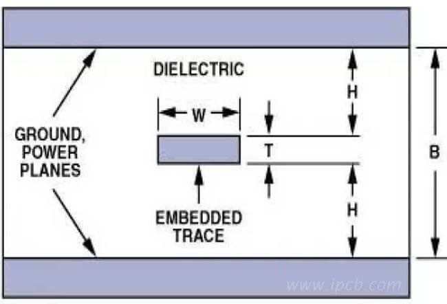
3.1 When a square wave of a signal moves forward with a high-level positive pressure signal in the signal line of the transmission line assembly, the reference layer (such as the ground layer) closest to it is theoretically necessary The negative pressure signal induced by the electric field accompanies the forward (equal to the return path of the positive pressure signal), so that the overall loop system can be completed. If the "signal" travels forward and freezes its flight time for a short time, you can imagine the instantaneous impedance (Instantanious Impedance) that the signal line, dielectric layer, and reference layer will experience together. This is the so-called "Characteristic impedance".
Therefore, the "characteristic impedance" should be related to the line width (w), line thickness (t), dielectric thickness (h) and dielectric constant (Dk) of the signal line. The microstrip line, one of the transmission lines, has the following diagram and calculation formula: [Note to the author] The correct translation of Dk (Dielectric Constant) should be the dielectric constant. In the original text...r should actually be called "relative capacitance" "Relative Permitivity" is right. The latter is to look at things from the standpoint of parallel metal plate capacitors. Because it is closer to the facts, many important specifications (such as IPC-6012, IPC-4101, IPC-2141 and IEC-326) have been renamed... r in recent years. And the E in the original picture is incorrect, it should be a Greek letter (Episolon).
3.2 Consequences of poor impedance matching
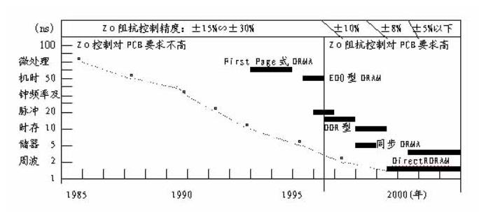
Since the original term "characteristic impedance" (Z0) of high-frequency signals is very long, it is generally referred to as "impedance". Readers must be careful, this is not exactly the same as the impedance value (Z) that appears in the low-frequency AC (60Hz) wire (not the transmission line). In digital systems, when the Z0 of the entire transmission line can be managed properly, and if it is controlled within a certain range (±10% or ±5%), this high-quality transmission line will reduce noise and avoid misoperation. However, when any one of the four variables (w, t, h, r) of Z0 in the above microstrip line is abnormal, such as a gap in the signal line in the figure, the original Z0 will rise suddenly (see the above formula The fact that Z0 is inversely proportional to W), and cannot continue to maintain the due stability and uniformity (Continuous), the energy of the signal will inevitably advance partly, while part of the rebound reflection is missing. In this way, noise and malfunction cannot be avoided. The hose in the picture below was suddenly stepped on by Yamazaki's son, causing abnormalities at both ends of the hose, which just illustrates the above-mentioned problem of poor characteristic impedance matching.

3.3 Poor impedance matching causes noise
The rebound of some of the signal energy mentioned above will cause the original good-quality square wave signal to be abnormally deformed immediately (that is, the Overshoot of the high level upward, the Undershoot of the low level downward, and the subsequent Ringing of the two; details See also TPCA Proceedings Issue 13 "Embedded Capacitors"). Such high-frequency noise can cause malfunctions when it is severe, and the faster the pulse speed, the more noise and the easier it is to make mistakes.
4. Test of characteristic impedance
4.1 Measurement with TDR
It can be seen from the above that the characteristic impedance value in the overall transmission line must not only maintain uniformity, but also make its value fall within the tolerance range required by the designer. The general measurement method is to use Time Domain Reflectometry (TDR). This TDR can generate a step wave (StepPulse or Step Wave) and send it into the transmission line to be tested to become an incident wave (Incident Wave). Therefore, when the width of the signal line changes, the ups and downs of the Z0 ohm value will also appear on the screen.
4.2 The low frequency does not need to measure Z0, the high speed will use TDR
When the wavelength of the signal square wave (lambda) far exceeds the length of the board circuit, there is no need to consider the troublesome issues in high-speed areas such as reflection and impedance control. For example, the CPU that was not fast in the early 1989 had a clock rate of only 10MHz, and of course there would be no complicated problems in signal transmission. However, the internal frequency of the current Pentium 4. is as high as 1.7GHz, which will naturally cause problems. Compared with the huge difference in the past, it is nothing more than a sky! From the wave formula, we can see that the wavelength of the 10MHz square wave mentioned above is:
But when the clock rate of the DRAM chipset has risen to 800MHz, the wavelength of its square wave will also be shortened to 37.5cm; and the speed of the P-4 CPU is as high as 1.7GHz and the wavelength is shorter to 17.6cm, so its PCB motherboard The external frequency transmitted between the above two will also be accelerated to the realm of 400MHz and 75cm wavelength. It can be seen that the line length in these packaged substrates (substrate), and even the line length on the mother board, have reached the signal wavelength. Of course, the transmission line effect must be paid attention to, and TDR measurement must also be used. .
4.3 TDR has a long history
Using a time domain reflectometer to measure the characteristic impedance (Z0) value of the transmission line is not a new thing. In the early years, it was used to monitor the safety of submarine cables, and always pay attention to whether there is a "disconnection" problem in transmission quality. Now it is gradually used in the field of high-speed computer and high-frequency communication.
4.4 TDR test of CPU carrier board
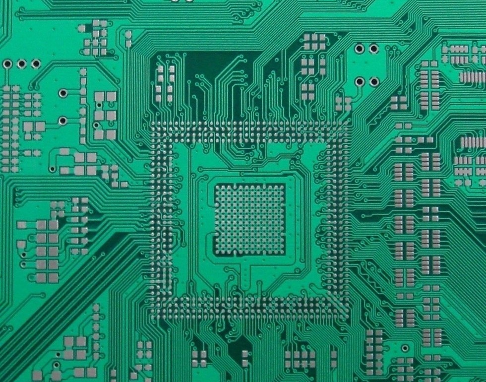
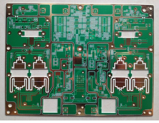
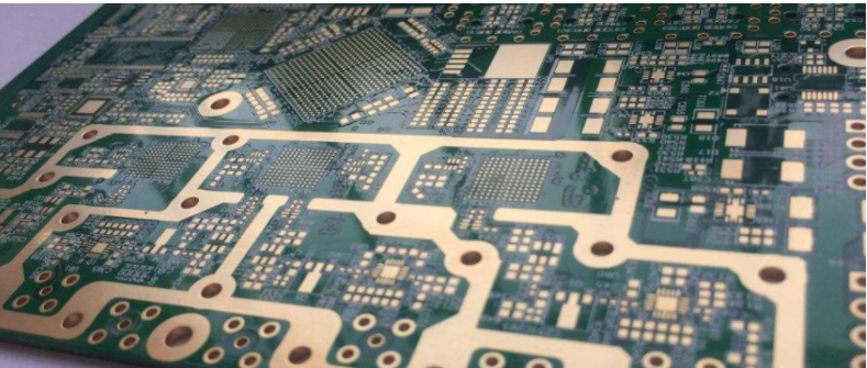
The packaging technology of active components has been continuously renovated and accelerated in recent years. The C-DIP and P-DIP double-row socket soldering (PTH) in the 1970s has almost disappeared. In the 1980s, the QFP (four-sided protruding foot) or PLCC (four-sided hook foot) of the metal tripod (Lead Frame) has gradually decreased from the HDI board or hand-held models. Instead, it is the BGA or CSP, or the LGA with no legs, which is the bottom surface of the organic sheet (Area Array). Even the interconnection of the chip (Chip) to the carrier (Substract) has progressed from wire bond to the shorter and more direct "flip chip" (FC) technology. The speed of the electronics industry's charge has almost changed rapidly!
Hioki launched the "1109 Hi Tester" at JPCA in June 2001. In order to correctly measure the Z0 of the 1.7GHz high-speed transmission FC/PGA carrier board, the flying probe is no longer used for rapid movement. SMA probe type TDR manual touch test (Press-type) is also abandoned. Instead, the fixed high-frequency short-distance cable is used for precise positioning with the fixed high-frequency stylus, and high-precision automatic testing is performed at the point where the automatic distance shift and contact line are to be measured. .
With the XY displacement of the CCD camera lens monitoring platform, and the laser height sensor inspecting the drop point in the Z direction, these dual precise positioning and point finding, coupled with the cooperation of the rotatable contact stylus, can avoid repetition. The trouble of using traditional cables, connectors, and switches, etc., greatly reduces the error of TDR measurement. This has made the "1109HiTESTER" measurement of Z0 on the package carrier board far more accurate than other methods.
In fact, the probe combination uses a four-directional probe set (each direction has 1 Signal and 2 Gnd respectively). When the CCD monitors and measures at the same time, the data will of course be more accurate. And any error caused by temperature changes can also be minimized under the automatic correction of the standard value ceramic card board.
4.5 Accurate and neat
This newly launched 1109 can not only perform Z0 measurement on the CPU of the highest-end packaged carrier board, but also perform precise measurements on the other high-priced CSP, BGA, FC, etc. with ease. The size to be tested can even be as small as 10mm*10mm, to a huge 500mm*600mm, and it can cope with drastic changes. In the future, the industry may also require measurement of Z0 for actual signal lines other than Coupon. This difficult TDR technology is currently under development.