When you try to stabilize the various signals on the board, signal integrity issues can cause some trouble. The IBIS model is a simple way to solve these problems. You can use the IBIS model to extract some important variables for signal integrity calculations and to find solutions forPCB design. The various values you extract from the IBIS model are an integral part of the signal integrity design calculations.
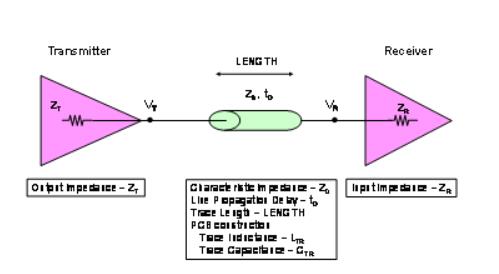
When you deal with transmission line matching problems in your system, you need to understand the electrical impedance and characteristics of integrated circuits and PCB lines. Figure 1 shows the structure of a single-ended transmission line.

Figure 1 Single-ended transmission line connecting transmitter, transmission line and receiver components
As far as the transmission line is concerned, we can extract the IC's transmitter output impedance (ZT, Ω) and receiver input impedance (ZR, Ω) from the IC IBIS model. Many times, the IC manufacturer’s product specifications do not describe these integrated circuit (IC) specifications, but you can get all these values through the IBIS model.
You can define the transmission line with the following four parameters: characteristic impedance (Z0, Ω), board propagation delay (D, ps/in), line propagation delay (tD, seconds), and trace length (LENGTH, inches). Generally speaking, the Z0 range of the FR-4 board is 50Ω to 75Ω, and the D range is 140 ps/in to 180 ps/in. The actual values of Z0 and D depend on the material and physical dimensions of the actual transmission line ("Reference 1"). The line delay (tD) on a particular circuit board is equal to the propagation delay (D) multiplied by the length of the trace you are using (LENGTH). The calculation methods for all boards are:
D = 1012 Ö (CTR * LTR) or
D = 85 ps/in * Ö (er)
Z0 = Ö(LTR/CTR)
tD = D * LENGTH
When using the FR-4 board, the reasonable stripline propagation delay is 178 ps/inch, and the characteristic impedance is 50Ω.
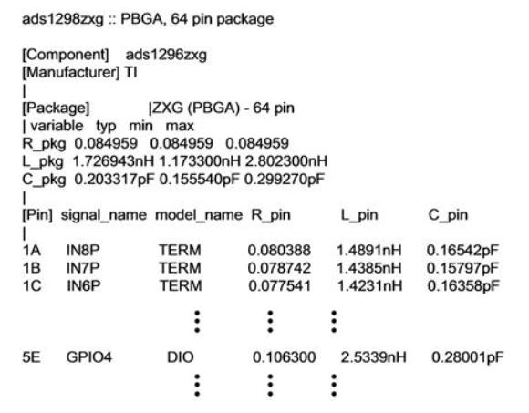
The transmitter specification used for signal integrity evaluation is the output impedance (ZT). When determining the output impedance, the [Pin] area in the IBIS model provides the parasitic value of the resistance, inductance, and capacitance of each pin. After that, you can put the package capacitance and the capacitance value (C_comp) of each buffer together for a clearer understanding.
As described in [Component], [Manufacturer] and [Package] above the [Pin] keyword, the [Pin] keyword is related to the specific package. You will find package capacitance and inductance in the [Pin] keyword table because it is related to the pin. For example, in the ads129x.ibs model ("Reference 2"), Figure 2 shows where to find the L_pin value and C_pin value of pin 5E (PBGA, 64-pin package) signal GPIO4.

Figure 2 Package list of ads1296zxg package including C_pin value
The signal and package L_pin (pin inductance) and C_pin (pin capacitance) are 1.489 Nh and 0.28001 pF, respectively.
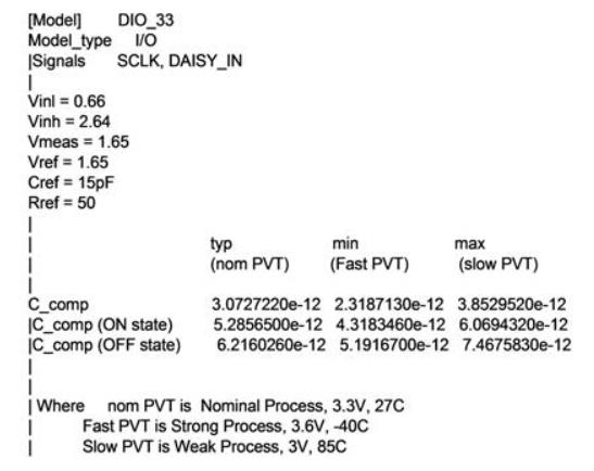
The second important capacitance value is the C_comp value under the [Model] keyword. Just as you find the correct model in the IBIS model, you will also find a list of C_comp values. Figure 3 shows an example of C_comp in the DIO_33 model ("Reference 2").

Figure 3 In ads129x.ibs, it is a list of Model DIO_33 and its related C_comp values.
In the declaration in Figure 3, the "|" symbol indicates a comment. The list of valid C_comp ("Reference 3") in this statement is:
| typ min max
| (nom PVT) (Fast PVT) (slow PVT)
C_comp 3.0727220e-12 2.3187130e-12 3.8529520e-12
Through this list, PCB designers can choose among three values. In the PCB transmission line design stage, the typical value of 3.072722 Pf is the correct choice.
The IBIS model provides some clues for PCB designers, allowing them to simulate the board before moving on to the prototype design. If you know the search method, the IBIS model can provide you with the characteristic impedance and capacitance of all pins. The next step in the evaluation is to determine the input/output resistance of each buffer, which we will introduce next time.