People in the industry are more aware of the impact of PCB board warpage when making PCB boards. For example, it prevents the installation of SMT electronic components, or the electronic components (including integrated blocks) have poor contact with the solder joints of the printed PCB board, or when the electronic components are installed, some feet cannot be cut or will be cut to the substrate; during wave soldering In some parts of the substrate, the pads cannot touch the solder surface and the tin cannot be soldered, etc.;
One aspect of the cause of the warpage of the printed PCB board is that the substrate (copper clad laminate) used may be warped. However, during the processing of the printed PCB board, due to thermal stress, chemical factors, and improper production processes will also cause printing. The PCB board is warped.
Therefore, for the printed PCB board factory, the first thing is to prevent the printed PCB board from warping during the processing; and then there must be a suitable and effective treatment method for the PCB board that has already warped.
1. Prevent printed PCB board from warping during processing
1. Prevent or increase the warpage of the substrate due to improper inventory method
(1) Since the copper clad laminate is in the storage process, because moisture absorption will increase the warpage, the moisture absorption area of the single-sided copper clad laminate is large. If the inventory environment humidity is high, the single-sided copper clad laminate will significantly increase the warpage. The moisture of double-sided copper clad laminate can only penetrate from the end surface of the product, the moisture absorption area is small, and the warpage changes slowly. Therefore, for the copper clad laminates without moisture-proof packaging, attention should be paid to the warehouse conditions, minimize the humidity in the warehouse and avoid bare copper clad laminates to avoid increased warpage of the copper clad laminates in storage.
(2) Improper placement of copper clad laminates will increase warpage. Such as vertical placement or heavy objects on the copper clad laminate, improper placement, etc. will increase the warpage and deformation of the copper clad laminate.
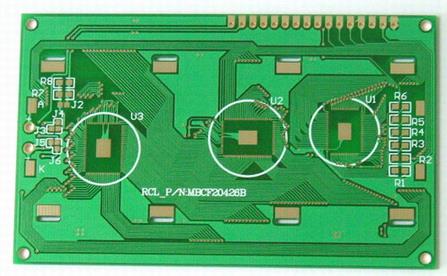
Soldered PCBA
2. Avoid warping caused by improper printed PCB board circuit design or improper processing technology.
For example, the conductive circuit pattern of the PCB board is not balanced or the PCB
The lines on both sides of the board are obviously asymmetrical, and there is a large area of copper on one side, which forms a large stress, which causes the PCB to warp. The high processing temperature or large thermal shock in the PCB manufacturing process will cause the PCB to warp. For the impact caused by improper storage method of superstrate, PCB factory is better to solve it, and it is enough to improve the storage environment and eliminate vertical placement and avoid heavy pressure. For PCB boards with a large area of copper in the circuit pattern, it is best to mesh the copper foil to reduce stress.
3. Eliminate substrate stress and reduce PCB board warpage during processing
In the process of PCB processing, the substrate has to be subjected to heat and many kinds of chemical substances many times. For example, after the substrate is etched, it needs to be washed with water, dried and heated. Electroplating is hot during pattern plating. After printing green oil and marking characters, it must be heated or dried with UV light. Thermal shock to the substrate when hot air is sprayed. It's also very big and so on. These processes may cause the PCB board to warp.
4. When wave soldering or dip soldering, the solder temperature is too high and the operation time is too long, which will increase the warpage of the substrate. For the improvement of the wave soldering process, the electronic assembly factory needs to cooperate.
Since stress is the main cause of substrate warpage, if the copper clad laminate (also called h board) is baked before the copper clad laminate is put into use, many PCB manufacturers believe that this approach is beneficial to reduce the warpage of the PCB board. The function of the baking sheet is to fully relax the stress of the substrate, thereby reducing the warpage and deformation of the substrate during the PCB manufacturing process.
The method of h board is: conditional PCB factories use large oven h board. Put a large stack of copper clad laminates into the oven before production, and bake the copper clad laminates for several to ten hours at a temperature near the glass transition temperature of the substrate. The PCB board produced by the copper clad laminate of the h board has relatively small warpage deformation, and the product qualification rate is much higher. For some small PCB
In the factory, if there is not such a large oven, the substrate can be cut into small pieces and then bake, but there should be a heavy object to press the plate when baking the plate, so that the substrate can be kept flat during the stress relaxation process. The temperature of the baking sheet should not be too high, because the substrate will change color if the temperature is too high. It should not be too low, and it takes a long time for the temperature to be too low to relax the substrate stress.
Second, the printed PCB board warpage leveling method
1. Level the warped board in time during the PCB manufacturing process
In the PCB manufacturing process, pick out the board with a relatively large warpage and level it with a roller leveling machine, and then put it into the next process. Many PCB manufacturers believe that this approach is effective in reducing the warpage ratio of PCB finished boards.
2. PCB finished board warping leveling method
For the PCB boards that have been completed, the warpage is obviously out of tolerance, and cannot be leveled with a roller leveling machine, some PCB factories put it in a small press (or similar fixture) to press the warped PCB board Live for a few hours to more than ten hours for cold pressing and leveling. Observed from practical applications, the effect of this practice is not very obvious. One is that the leveling effect is not great, and the other is that the leveled board is easy to rebound (that is, the warpage is restored).
Some PCB factories heat the small press to a certain temperature, and then treat the warped PCB
Hot pressing and leveling of the board will have better effect than cold pressing, but if the pressure is too high, the wire will be deformed; if the temperature is too high, it will cause defects such as discoloration of rosin perfume and discoloration of the base. Moreover, it takes a long time (several hours to ten hours) to see the effect whether it is cold press leveling or hot press leveling, and the proportion of warpage rebound of the leveled PCB board is also relatively high. Is there a better leveling method?
3. Hot pressing and leveling method for warped PCB board arch mold
According to the mechanical properties of polymer materials and years of work practice, this article recommends the hot-pressing and leveling method of the bow-shaped mold. According to the area of the PCB to be leveled, a number of very simple bow-shaped molds are made. Here is a leveling operation method:
Clamp the warped PCB board into the bow-shaped mold and put it into the oven to bake and level:
Place the warped PCB board's warped surface against the mold bow curve, adjust the clamp screw to make the PCB board slightly deform in the opposite direction of its warpage, and then put the mold with the PCB board in an oven heated to a certain temperature for baking Bake for a while. Under heated conditions, the substrate stress gradually relaxes, so that the deformed PCB board is restored to a flat state. But the baking temperature should not be too high, so as to avoid the discoloration of the rosin perfume or the yellowing of the substrate. But the temperature should not be too low. It takes a long time to fully relax the stress at a lower temperature.