The following considerations are often taken into account when designing PCB components.
1. Does PCB board shape match the whole machine?
2. Is the spacing between components reasonable? Is there a level or level of conflict?
3. Does PCB need to be made up? Is the process edge reserved? Are mounting holes reserved? How to arrange the positioning holes?
4. How to place and heat the power module?

5. Is it convenient to replace the components that need to be replaced frequently? Are adjustable components easy to adjust?
6. Is the distance between the thermal element and the heating element considered?
7. How is the EMC performance of the whole board? How can layout effectively enhance anti-interference ability?
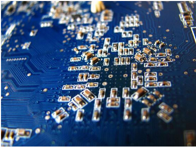
For the problem of the spacing between components and components, based on the distance requirements of different packages and the characteristics of Altium Designer itself, if the constraint is set by rules, the setting is too complicated and difficult to achieve. A line is drawn on the mechanical layer to indicate the outer dimensions of the components, as shown in Figure 9-1, so that when other components approach, the approximate spacing is known. This is very practical for beginners, but also enable beginners to develop good PCB design habits.
Based on the above considerations and analysis, common PCB layout constraint principles can be classified as follows.
Element arrangement principle
1. Under normal conditions, all components should be arranged on the same surface of the PCB. Only when the top component is too dense, some components with limited height and low calorific value (such as chip resistance, chip capacitance, chip IC, etc.) can be placed on the bottom layer.
2. On the premise of ensuring the electrical performance, the components should be placed on the grid and arranged parallel or vertically to each other in order to be neat and beautiful. Under normal circumstances, components are not allowed to overlap, the arrangement of components should be compact, input components and output components as far as possible apart from each other, do not appear crossover.
3, there may be high voltage between some components or wires, should increase their distance, so as not to cause accidental short circuit due to discharge, breakdown, layout as much as possible to pay attention to the layout of these signals space.
4. Components with high voltage should be arranged as far as possible in places not easily accessible by hand during debugging.
5. located at the edge of the plate components, should try to do two plate thickness from the edge of the plate.
6. components should be evenly distributed on the whole board, not this area dense, another area loose, improve the reliability of the product.
Follow the layout principle of signal direction
1. After placing the fixed components, arrange the position of each functional circuit unit one by one according to the direction of the signal, take the components of each functional circuit as the center, and carry out local layout around it.
2. The layout of components should be convenient for signal flow, so that the signal keeps the same direction as far as possible. In most cases, the signal flow is arranged from left to right or from top to bottom, and components directly connected to input and output terminals should be placed near input and output connectors or connectors.
Prevention of electromagnetic interference
Constraints on PCB component layout
(1) For components with strong radiation electromagnetic fields and components with high sensitivity to electromagnetic induction, the distance between them should be increased, or a shielding cover should be considered for shielding.
(2) Try to avoid high and low voltage components mixed with each other and strong and weak signal components interlaced together.
(3) for components that will produce magnetic fields, such as transformers, loudspeakers, inductors, etc., attention should be paid to reducing the cutting of magnetic lines on printed wires when layout, and the magnetic field direction of adjacent components should be perpendicular to each other to reduce the coupling between each other.
he arrangement of inductors 90° perpendicular to the inductor.
(4) Shielding interference sources or easily disturbed modules, shielding cover should be well grounded.
Suppression of thermal interference
(1) Heat generating elements should be placed in a position conducive to heat dissipation. If necessary, a separate radiator or small fan can be set to lower the temperature and reduce the impact on neighboring components.
(2) Some high-power integrated blocks, high-power tubes, resistors, etc., should be arranged in places where heat dissipation is easy, and separated from other components by a certain distance.
(3) The thermal sensitive element should be close to the measured element and away from the high temperature area, so as not to be affected by other heating power equivalent elements and cause misoperation.
(4) When the element is placed on both sides, the heating element is generally not placed on the bottom layer.
Principle of adjustable component layout
The layout of adjustable components such as potentiometers, variable capacitors, adjustable inductance coils and micro-switches should consider the structural requirements of the whole machine: if the machine is adjusted outside, its position should be adapted to the position of the adjusting knob on the chassis panel; In case of in-machine adjustment, it should be placed on the PCB where it is easy to adjust.