Due to the complex process flow of PCB manufacturing, in the planning and construction of intelligent manufacturing, it is necessary to consider the related work of process and management, and then carry out automation, information and intelligent layout.
1
Process classification
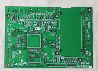
According to the number of PCB layers, it is divided into single-sided, double-sided, and multi-layer boards. The three board processes are not the same.
There is no inner layer process for single-sided and double-sided panels, basically cutting-drilling-follow-up process.
Multilayer boards will have internal processes
1) Single panel process flow
Cutting and edging - drilling - outer layer graphics - (full board gold plating) - etching - inspection - silk screen solder mask - (hot air leveling) - silk screen characters - shape processing - testing - inspection
2) Process flow of double-sided tin spraying board
Cutting edge grinding - drilling - heavy copper thickening - outer layer graphics - tin plating, etching tin removal - secondary drilling - inspection - screen printing solder mask - gold-plated plug - hot air leveling - silk screen characters - shape processing - testing - test
3) Double-sided nickel-gold plating process
Cutting edge grinding - drilling - heavy copper thickening - outer layer graphics - nickel plating, gold removal and etching - secondary drilling - inspection - silk screen solder mask - silk screen characters - shape processing - test - inspection

4) Process flow of multi-layer board tin spraying board
Cutting and grinding - drilling positioning holes - inner layer graphics - inner layer etching - inspection - blackening - lamination - drilling - heavy copper thickening - outer layer graphics - tin plating, etching tin removal - secondary drilling - inspection -Silk screen solder mask-Gold-plated plug-Hot air leveling-Silk screen characters-Shape processing-Test-Inspection
5) Process flow of nickel-gold plating on multilayer boards
Cutting and grinding - drilling positioning holes - inner layer graphics - inner layer etching - inspection - blackening - lamination - drilling - heavy copper thickening - outer layer graphics - gold plating, film removal and etching - secondary drilling - inspection - Screen printing solder mask-screen printing characters-shape processing-testing-inspection
6) Process flow of multi-layer plate immersion nickel-gold plate
Cutting and grinding - drilling positioning holes - inner layer graphics - inner layer etching - inspection - blackening - lamination - drilling - heavy copper thickening - outer layer graphics - tin plating, etching tin removal - secondary drilling - inspection -Silk screen solder mask-Chemical Immersion Nickel Gold-Silk screen characters-Shape processing-Test-Inspection.
2
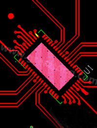
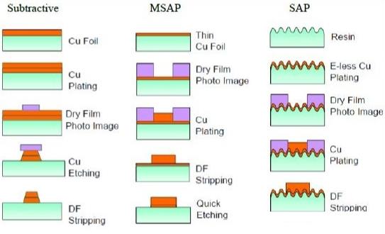
Inner layer production (graphic transfer)
Inner layer: cutting board, inner layer pre-processing, laminating, exposure, DES connection
Cutting (Board Cut)
1) Cutting board
Purpose: Cut the large material into the size specified by MI according to the requirements of the order (cut the substrate material to the size required by the work according to the planning requirements of the pre-production design)
Main raw materials: base plate, saw blade
The base plate is made of copper sheet and insulation lamination. There are different thickness specifications according to the requirements. According to the copper thickness, it can be divided into H/H, 1OZ/1OZ, 2OZ/2OZ, etc.
Precautions:
a. To avoid the influence of the board edge barry on the quality, after cutting, perform edge grinding and fillet treatment
b. Considering the impact of expansion and contraction, the cutting board is baked before being sent to the process
c. Cutting must pay attention to the principle of consistent mechanical direction
Edging/rounding: mechanical polishing is used to remove the glass fibers left by the right angles of the four sides of the board during cutting, so as to reduce scratches/scratches on the board surface in the subsequent production process, which may cause quality hazards
Baking plate: remove water vapor and organic volatiles by baking, release internal stress, promote cross-linking reaction, and increase the dimensional stability, chemical stability and mechanical strength of the plate
Control points:
Sheet material: puzzle size, sheet thickness, sheet material type, copper thickness
Operation: baking time/temperature, stacking height
(2) Production of inner layer after cutting board
Function and principle:
The inner copper plate roughened by the grinding plate is dried by the grinding plate, and the dry film IW is attached, and then irradiated with UV light (ultraviolet rays). The exposed dry film becomes hard and cannot be dissolved in weak alkali, but can be dissolved in strong alkali. The unexposed part can be dissolved in weak alkali, and the inner layer circuit is to use the characteristics of the material to transfer the graphics to the copper surface, that is, image transfer.
Detail :(The photosensitive initiator in the resist in the exposed area absorbs photons and decomposes into free radicals. The free radicals initiate a cross-linking reaction of monomers to form a spatial network macromolecular structure that is insoluble in dilute alkali. It is soluble in dilute alkali when the reaction occurs.
The two have different dissolving properties in the same solution to transfer the pattern designed on the negative to the substrate to complete the image transfer).
The circuit pattern has higher requirements for temperature and humidity conditions, generally requiring a temperature of 22+/-3 degree Celsius and a humidity of 55+/-10% to prevent the deformation of the film. The dust in the air is required to be high. With the increase in the density of the lines and the smaller the lines, the dust content is less than or equal to 10,000 or more.
Material introduction:
Dry film: Dry film photoresist for short is a water-soluble resist film. The thickness is generally 1.2mil, 1.5mil and 2mil. It is divided into three layers: polyester protective film, polyethylene diaphragm and photosensitive film. The function of the polyethylene diaphragm is to prevent the soft film barrier agent from sticking to the surface of the polyethylene protective film during the transportation and storage time of the roll-shaped dry film. The protective film can prevent the oxygen from penetrating into the barrier layer and the free radicals in it from accidentally reacting to cause the photopolymerization reaction, and the dry film that has not been polymerized is easily washed away by the sodium carbonate solution.
Wet film: Wet film is a one-component liquid photosensitive film, which is mainly composed of high photosensitive resin, sensitizer, pigment, filler and a small amount of solvent. The production viscosity is 10-15dpa.s, and it has corrosion resistance and electroplating resistance., Wet film coating methods include screen printing, spraying and other methods.
Products: Electronic products cover multilayer boards, high-density interconnect HDI, high-frequency high-speed boards, flexible circuit boards, rigid-flex circuit boards and other special-specification boards (including: metal substrates, thick copper boards, ultra-long boards, ceramics Board etc.).