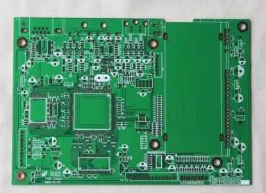
HDI board is one of the most precise circuit boards, and its board manufacturing process is also the most complicated. Its core steps mainly include the formation of high-precision printed circuits, the processing of micro-vias, and the electroplating of surfaces and holes. The following are the core steps in HDI PCB plate making.
1. Ultra-fine circuit processing
With the development of science and technology, some high-tech equipment is becoming more and more miniaturized and sophisticated, which requires higher and higher HDI boards.
The line width/line spacing of some devices has evolved from the early 0.13 mm (5 mil) to 0.075 mm (3 mil), and has become the mainstream standard. As a leading company in the HDI Allegro industry, Shenzhen Benqiang Circuit Co., Ltd.'s related production process has reached 38μm (1.5 mil), which has approached the industry's limit.
Increasing line width/line spacing requirements have brought the most direct challenge to the graphics imaging in the PCB manufacturing process. So how are the copper wires on these precision boards formed?
The current formation process of refined circuits includes laser imaging (pattern transfer) and pattern etching.
The laser direct imaging (LDI) technology is to directly scan the surface of the copper clad laminate with photoresist to obtain the refined circuit pattern. The laser imaging technology greatly simplifies the process flow and has become the mainstream in HDI PCB plate making. Process technology.

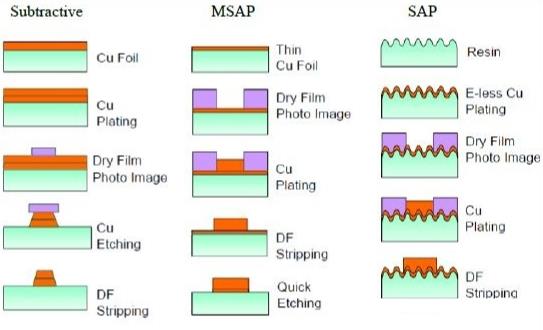
Now the semi-additive method (SAP) and the improved semi-additive method (mSAP) are more and more used, that is, the pattern etching method. This technical process can also realize conductive lines with a line width of 5um.
2. Micro-hole processing
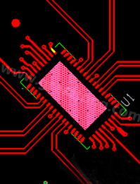
The important feature of HDI circuit boards is that they have micro vias (aperture ≤0.10 mm), and these holes are buried blind via structures.
The holes on the HDI board are currently mainly processed by laser, but there are also CNC drilling.
Compared with laser drilling, mechanism drilling also has its own advantages. When laser processing the through hole of the epoxy glass cloth dielectric layer, the quality of the hole will be slightly worse due to the difference in the ablation rate between the glass fiber and the surrounding resin, and the remaining glass fiber filaments on the hole wall will affect the reliability of the through hole . Therefore, the superiority of mechanical drilling at this time is reflected. In order to improve the reliability and drilling efficiency of PCB boards, laser drilling and mechanical drilling technologies have been steadily improved.
3. Electroplating and surface finishing
How to improve the uniformity and deep hole plating ability in PCB manufacturing, and improve the reliability of the board. This depends on the continuous improvement of the electroplating process, starting from many aspects such as the proportion of the electroplating solution, equipment deployment, and operating procedures.
High-frequency sound waves can accelerate the etching ability; permanganic acid solution can enhance the ability of the workpiece to decontaminate. The high-frequency sound waves will stir and add a certain proportion of potassium permanganate electroplating solution in the electroplating tank. This helps the plating solution flow evenly into the holes. Thereby improving the deposition ability of electroplated copper and the uniformity of electroplating.
At present, the copper-plated hole filling of blind holes is also mature, and copper filling of through holes with different apertures can be carried out. The two-step copper plated hole filling can be suitable for through holes with different apertures and high thickness-to-diameter ratios. It has a strong copper filling ability and can minimize the thickness of the surface copper layer.
There are many options for the final surface finish of the PCB. Electroless nickel/gold (ENIG) and electroless nickel/palladium/gold (ENEPIG) are commonly used on high-end PCBs.