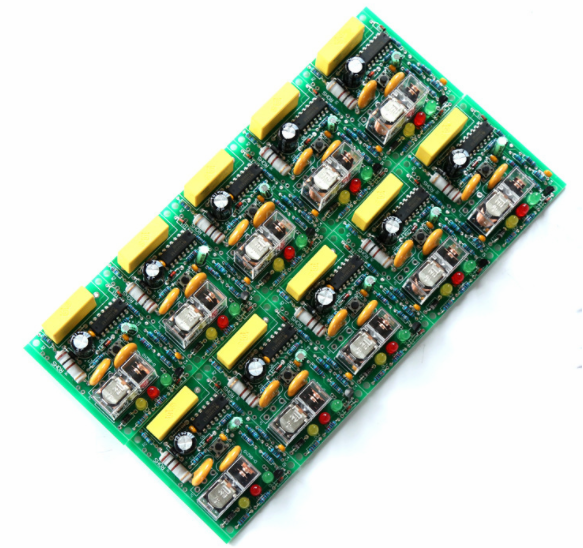
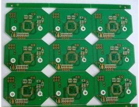
One, talk about the experience of PCB copper cladding in the circuit board
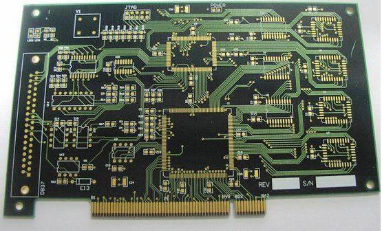
The so-called copper cladding is based on the free space of the PCB and then filled with solid copper. These copper areas are also called copper filling. The important significance of copper plating is to reduce the ground impedance, improve the anti-interference ability, reduce the voltage drop, improve the power supply efficiency, and connect with the ground wire to reduce the loop area. If the PCB has more pads, such as Sgnd, Agnd, GND, etc., how to cover the copper? My method is to use the most important "foundation" as a reference for independent copper according to the different positions of the PCB board, and separate digital and analog to apply copper from many words. At the same time as the copper cladding, the first corresponding power connection in bold: V5.0V, V3.6V, V3.3V, etc.

As a result, many deformable structures of different shapes are formed. The copper cladding needs to deal with several problems: one is different single-point connections, and the practice is to connect through 0 ohm resistance or magnetic beads or inductance, and the second is the crystal near the copper cladding. The circuit for crystal vibration is high-frequency emission The source, the practice is to apply copper around the crystal, and then the crystal vibration of the shell is grounded in other ways.
Third, the island (dead zone) problem, if it feels very large, then there is not much to define a hole. In addition, large-area copper or mesh-clad copper is good, and it is not easy to promote. why is that? Large area copper cladding, if wave soldering, the board may tilt upwards, or even blisters. From this perspective, the heat dissipation effect of the power grid is better. It is usually a high-frequency circuit to cope with the interference requirements of a multi-purpose power grid. The low-frequency circuit has a large current circuit and other commonly used all-copper circuits.
2. Points for Attention in Converting CAD Files to Gerber Files
(I), Protel for Windows transfer to Gerber should be aware of the problem
1. PFW can automatically generate D code tables based on PCB files.
However, there may be as many as hundreds of D codes in the D code table, and you should know exactly the D code capacity of the optical drawing system.
2. If PFW does not automatically generate D code tables, the following situations may cause errors:
1. There may be 0 pads or wire sizes in PFW;
2. With embossed welding plate;
When 3. D code is not configured.
In these cases, a large D code will appear in the mat file. 3. PFW has a long octagonal pad, and there should be no such D code in the conversion of the D code table. Since this definition is not accepted in most current optical drawing systems, the existence of the D code may cause errors.
In this case, you should use the Fill method to match this D code.
4. It is better to use user-defined D code table instead of using PFW to automatically generate D code table.
(Ii) Problems that should be paid attention to when transferring Protel for DOS to Gerber
1. The upper and lower limits of D code matching should not be set too wide, which will easily cause too much deviation and cause the minimum distance to be unguaranteed. 2. Sometimes the filling area (filling) conversion may cause confusion.
At this time, all the Chinese type D codes in the D code table should be deleted, and then converted again.
3. When the D code does not match and manual matching is required, mode 3 must be selected.
4. In the arc (ARC) conversion, the step distance (arc quality) should not be set too small, otherwise it will cause too much data and the arc edge is not smooth.
5. Resistance welding expansion value can be negative.
6. ARC conversion can choose arc description or straight line description.
Software arc: on is described by a straight line, and the polyline is close to the garden arc during conversion.
Software arc: Closing is the description of the arc, the description of the real garden arc. It is best to use the arc description of an optical plotter that can accept arc descriptions.
This makes Gerber files have a small amount of data, and the edges of the light drawing arcs are smooth.
7. When the D code used exceeds 24, the G54 option should be turned on.
8. When the single-sided pad needs to be punched, open the Pad Holes item of the Optionssingle layer.
9. Some tool software can be generated by fully configuring the D code table through the mat file.
(C) PowerPCB should pay attention to problems when transferring Gerber.
1. After conversion, there are POWERPCB files that need to be filled with copper.
2. PowerPCB is a Windows version of the software, so the mat is basically the same during file conversion. The same problem is also to pay attention to which elements are selected in each drawing to avoid incorrect graphics errors caused by transfer.
(Iv) PADS should pay attention to problems when transferring Gerber.
1. PADS preset D code table D code capacity is too small, need to expand its capacity.
2. After the conversion, there is a gasket file that needs to be filled with copper. 3. Due to the particularity of the design line of the pad software, we need to pay attention to which elements are selected in each drawing to avoid errors caused by incorrect transfer of graphics.