PCB current load capacity in principle depends on the cross-sectional area and temperature rise of the copper section of the trace, but the cross-sectional area is positively related to the width and thickness of the circuit, but whether the current load capacity is directly proportional to the cross-sectional area of the copper wire may be Not necessarily anymore?
Assuming that under the same temperature rise of 10°C, a 1oz trace with a line width of 10mils can withstand a current of 1Amp, we should be sure that a trace with a line width of 50mils can withstand a current greater than 1Amp, but Will it be 5Amps in multiples? The answer seems to be no. First, refer to the MIL-STD-275 table, the maximum current it can withstand is actually only 2.6Amps.
PCB copper foil thickness-ounce (ounce, oz)
Generally, the thickness of copper foil used in PCB industry is "ounces (oz)", but "ounces" is obviously weight, how can it become thickness again? This is because in the terminology of copper skin, "ounce" has been converted into a unit of thickness. The more you listen to it, the more confused it becomes? This is because the specifications of copper sheets are defined by a few ounces (oz) per square inch (ft2), so we often say that 1oz (ounce) is 1oz weight per square inch (ft2). The thicker the copper skin, the heavier it is. Because the weight of the copper skin is proportional to the thickness, the ounce of the copper skin can be equal to the thickness and can be converted into millimeters (mm) or milli-inches (mils). This is actually a bit similar to using pounds to calculate when we calculate paper. If you are interested, check it out for yourself!

Here are a few commonly used sizes and converted to mils (millimeters) and mm (millimeters) for your reference:
0.5 ounce (oz) = 0.0007 inch (inch) = 0.7 mils = 0.018 millimeter (mm)
1.0 ounce (oz) = 0.0014 inch (inch) = 1.4 mils = 0.035 millimeter (mm)
2.0 ounces (oz) = 0.0034 inches (inch) = 2.8 mils = 0.070 millimeters (mm)
Let’s also try to calculate for you why 1oz of copper foil is approximately equal to 1.4mils:
The specific gravity of copper is 8.9 (gm/cm3),
Unit conversion: 1(ft2)=93055 (mm2), 1(mil)=2.54(um), 1(oz)=28.34(gm)
1oz volume = 28.34(gm) / 8.9(gm/cm3) = 3.1842(cm3) = 3184.2(mm3)
1oz thickness = 3184.2(mm3) / 93055(mm2) = 0.03422(mm) = 1.35 (mils)
Note: The density of copper foil will have different densities due to the use of different copper, so there may be some small errors in the calculation.
The relationship between PCB copper foil cross-sectional area, maximum load current and temperature rise
According to IPC-2221 Section 6.2 (Conductive Material Requirements), the maximum current carrying capacity (Current Carrying Capacity) of the circuit board can be divided into two types: inner circuit and outer circuit, and the maximum current of the inner circuit The current-carrying capacity is set to only half of the outer circuit. Here is an excerpt from Chart 6-4 of IPC-2221 to illustrate the relationship between the cross-sectional area, temperature rise, and maximum current carrying capacity of the copper foil of the external conductors and internal conductors.
In addition, someone cleverly summarized the relationship between the PCB circuit's current carrying capacity in the above chart and concluded a formula. This formula can be roughly used to replace the look-up table:
I = K△T0.44A0.75
K: is the correction factor, generally 0.024 for the inner layer of the copper clad wire, and 0.048 for the outer layer.
△T: is the maximum temperature difference, which means the temperature of the copper foil is higher than the surrounding environment after it is energized, the unit is degrees Celsius (°C)
(Some netizens questioned that there may be a problem with the interpretation of the △T temperature difference. It is currently being studied and clarified. If you have experience, please feel free to explain. Now it has been revised. If there is still something wrong, please correct me.)
A: is the cross-sectional area of the copper clad circuit, the unit is square milliinch (mil2)
I: is the maximum current carrying capacity (Current Carrying Capacity), the unit is ampere (Amp)
1(mil) = 25.4(um)
Although there are formulas that can directly calculate the maximum current load capacity of copper foil, it is not so simple when designing the actual circuit. Because the current carrying capacity of Trace is not only related to the cross-sectional area and temperature of the copper foil, other things such as the number of components on the line, pads and vias are directly related.
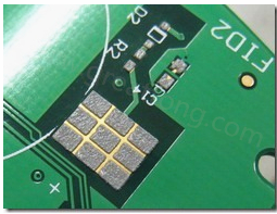
In the line segment with many solder pads (disks), the current carrying capacity of the line that eats tin after the furnace will be greatly increased. I believe many people should have seen the solder pads and soldering in some high-current boards. The reason why a certain section of the line between the pads is burned is very simple. This is because there is more solder on the pad, which increases the area on the line that can withstand current, and the line between the pad and the pad There is no change, so when the power is just turned on, or when the instruction is changed on the circuit, there is a good chance that the current surge will be too large. At this time, it is easy to burn the current between the pad and the pad. Lines with weaker carrying capacity.
The solution is to increase the width of the wire. If the board cannot allow the width of the wire to be increased, you can also consider opening the solder mask on the circuit that is easy to burn, and using the SMT process to add solder paste (solder paste). ), after reflow, the thickness of the wire can be increased, which also increases the current carrying capacity.
In this way, Lorry talked a lot. The main emphasis is that although the current carrying capacity of the PCB circuit has been calculated by looking up tables or formulas, these data are only calculated by straight lines, but in the actual PCB manufacturing, it must also be considered that the line may be contaminated by dust or debris, causing possible local line damage, so no matter what method we use to obtain the maximum current and line width that can be carried, it should be Also add a safety factor to prevent possible overload problems. A safety factor must be added to prevent possible overload problems. A safety factor must be added to prevent possible overload problems.
A safety factor must be added to prevent possible overload problems. A safety factor must be added to prevent possible overload problems. In addition, some lines should pay special attention to turning places. If there is an acute angle on the line, it may cause the problem of unsmooth current transmission. This may not be a problem for lines with small current or large line width, but if the line is When the current load tolerance is insufficient, problems are likely to occur. It's like a big car needs a relatively large turning radius when cornering, but a corner that is too right will make the car rush out of the track.