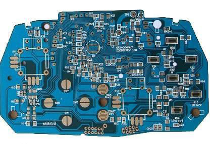
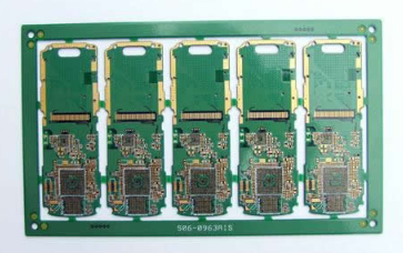
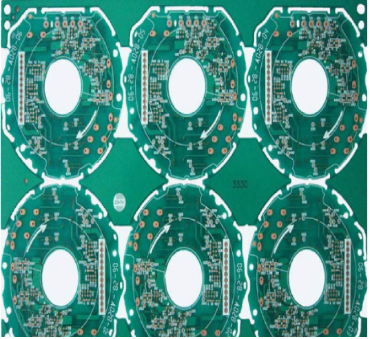
I. Overview
With the rapid development of microelectronics technology, PCB manufacturing is developing rapidly in the direction of multilayer, layered, functional and integrated. Promoting printed circuit design to adopt a large number of small holes, narrow pitches, and thin wires for circuit pattern conception and design, making printed circuit board manufacturing technology more difficult, especially the aspect ratio of multi-layer PCB board through holes exceeding 5:1 and The large number of deep blind holes used in the build-up board makes the conventional vertical electroplating process unable to meet the technical requirements for high-quality and high-reliability interconnection holes.
2. Introduction to the principle of horizontal electroplating
The method and principle of horizontal electroplating and vertical electroplating are the same, both must have both anode and cathode. After electrification, the electrode reaction will cause the main components of the electrolyte to ionize, and the charged positive ions will move to the negative phase of the electrode reaction zone; the charged negative ions will move to the electrode. The normal phase movement of the reaction zone produces metal deposition and gas evolution. Because the process of metal deposition at the cathode is divided into three steps: that is, the metal hydrated ions diffuse to the cathode; the second step is that the metal hydrated ions are gradually dehydrated when they pass through the electric double layer and adsorbed on the surface of the cathode; third The first step is that the metal ions adsorbed on the surface of the cathode accept electrons and enter the metal lattice.

The convection of the plating solution is produced by the use of external and internal mechanical stirring and pump stirring, the oscillation or rotation of the electrode itself, and the flow of the plating solution caused by the temperature difference. The closer to the surface of the solid electrode, the flow of the electroplating solution becomes slower and slower due to the influence of its frictional resistance. At this time, the convective flow rate on the surface of the solid electrode is zero. The rate gradient layer formed from the electrode surface to the convection plating solution is called the flow interface layer. The thickness of the flow interface layer is about ten times that of the diffusion layer, so the transport of ions in the diffusion layer is hardly affected by convection.
The key to printed circuit board plating is how to ensure the uniformity of the copper layer thickness on both sides of the substrate and the inner wall of the via. To obtain the uniformity of the plating layer thickness, it is necessary to ensure that the plating solution flow rate on both sides of the printed circuit board and the through holes is fast and consistent to obtain a thin and uniform diffusion layer. To achieve a thin and uniform diffusion layer, based on the current horizontal electroplating system structure, although many nozzles are installed in the system, the plating solution can be sprayed to the printed circuit board quickly and vertically to accelerate the plating solution in the through hole. The flow rate causes the plating solution to flow quickly, forming eddy currents on the upper and lower surfaces of the substrate and in the through holes, so that the diffusion layer is reduced and more uniform. However, usually when the plating solution suddenly flows into a narrow through hole, the plating solution at the entrance of the through hole will also have a reverse flow phenomenon. Coupled with the influence of the primary current distribution, it often causes the plating of the hole at the entrance., The thickness of the copper layer is too thick due to the tip effect, and the inner wall of the through hole constitutes a copper plating layer in the shape of a dog bone. According to the state of the plating solution flowing in the through hole, that is, the size of the eddy current and the reflow, and the state analysis of the quality of the conductive plating through hole, the control parameters can only be determined by the process test method to achieve the uniformity of the plating thickness of the printed circuit board. Because the size of the eddy current and the backflow still cannot be known by theoretical calculation methods, only the measured process method is used. From the measured results, it is known that to control the uniformity of the thickness of the copper electroplating layer of the through-hole, the controllable process parameters must be adjusted according to the aspect ratio of the PCB through-hole, and even a copper electroplating solution with high dispersibility must be selected and added Appropriate additives and improved power supply methods, namely the use of reverse pulse current for electroplating, can obtain copper coatings with high distribution capabilities.
3. Basic structure of horizontal electroplating system
According to the characteristics of horizontal electroplating, it is an electroplating method in which the printed circuit board is placed from a vertical type to a parallel plating liquid surface. At this time, the printed circuit board is the cathode, and some horizontal electroplating systems use conductive clamps and conductive rollers for current supply. From the convenience of the operating system, it is common to use the roller conductive supply method. The conductive roller in the horizontal electroplating system not only serves as the cathode, but also has the function of conveying the printed circuit board. Each conductive roller is equipped with a spring device, the purpose of which can be adapted to the electroplating needs of printed circuit boards of different thicknesses (0.10-5.00mm). However, during electroplating, all parts in contact with the plating solution may be plated with a copper layer, and the system will not work for a long time. Therefore, most of the currently manufactured horizontal electroplating systems design the cathodes to be switchable to anodes, and then use a set of auxiliary cathodes to electrolytically dissolve the copper on the plated rollers. For the sake of maintenance or replacement, the new electroplating design also considers the parts that are prone to wear and tear to facilitate removal or replacement. The anode is an array of adjustable size insoluble titanium baskets, which are respectively placed on the upper and lower positions of the printed circuit board. They are equipped with a spherical shape of 25mm in diameter and a phosphorous content of 0.004-0.006% soluble copper, cathodes and anodes. The distance between them is 40mm.
Fourth, the development advantages of PCB level plating
The development of PCB level plating technology is not accidental, but the need for special functions of high-density, high-precision, multi-function, and high-aspect ratio multilayer printed circuit board products is an inevitable result. Its advantage is that it is more advanced than the vertical rack plating process currently used, the product quality is more reliable, and large-scale production can be realized. Compared with the vertical electroplating process method, it has the following advantages:
(1) It is suitable for a wide range of sizes, no manual mounting is required, and all automatic operations are realized, which is extremely beneficial to improve and ensure that the operation process does not damage the surface of the substrate, and is extremely beneficial to the realization of large-scale large-scale production.
(2) In the process review, there is no need to leave a clamping position, which increases the practical area and greatly saves the loss of raw materials.
(3) Horizontal electroplating adopts full computer control to ensure the uniformity of the plating on the surface and holes of each printed circuit board under the same conditions of the substrate.