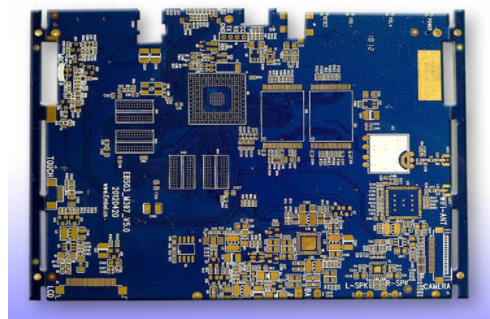
According to different equipment conditions, this article only applies to some PCB manufacturers.
one. PCB pad overlap
The overlap of PCB pads (except surface mount pads), that is, the overlapped placement of holes, will cause broken drills and wire damage when drilling multiple holes in one place.
two. Misuse of the graphics layer
1. Violation of conventional design, such as component surface design on the BOTTOM layer and welding surface design on the TOP, resulting in errors on the front and back of the file during file editing and the product is scrapped.
2. If there are slots that need to be milled in the PCB board, they should be drawn on the KEEPOUT LAYER or BOARD LAYER layer. No other layers or pads should be used to avoid mismilling or miss milling.
3. If there are holes on the double-sided PCB that do not need to be metallized, please specify separately.
three. Shaped hole
If there are irregular holes in the board, use the KEEPOUT layer to draw a filling area the same size as the hole. The length/width ratio of the special-shaped hole should be ≥2:3:1, and the width should be >1mm. Otherwise, the drilling machine will easily break the tool when processing the special-shaped hole, which will cause processing difficulties.

Four. Character placement
1. The characters cover the pad SMD soldering piece, which brings inconvenience to the continuity test of the printed board and the soldering of the components.
2. The character design is too small, which makes the screen printing difficult and makes the characters not clear enough. Character height≥30mil, width≥6mil.
five. Single-sided pad aperture setting
1. Single-sided pads are generally not drilled. If the drilling needs to be marked, the hole diameter should be designed to be zero. If the value is designed so that when the drilling data is generated, the hole will be drilled in the position, which will affect the appearance of the board, and the board will be scrapped.
2. If the single-sided pad needs to be drilled, a special mark must be made.
six. Draw pads with filled blocks
Drawing pads with filler blocks can pass the DRC inspection when designing the circuit, but it is not good for processing. Therefore, the solder mask data cannot be directly generated by the similar pads. When the solder resist is applied, the area of the filler block will be covered by the solder resist, resulting in the device Difficulty in welding.
seven. There are too many filler blocks in the design or the filler blocks are filled with very thin lines
1. The light drawing data is lost, the light drawing data is incomplete, and the light drawing is deformed.
2. Because the filling blocks are drawn one by one with lines during light drawing data processing, the amount of light drawing data generated is quite large, which increases the difficulty of data processing.
Eight. Surface mount device pad is too short
This is for continuity testing. For surface mount devices that are too dense, the spacing between the two pins is quite small, and the pads are also quite thin. The installation test must be staggered up and down (left and right), such as the pad design is too small. Short, although it does not affect the placement of the device, but it will make the test pin staggered.
Nine. The spacing of the large area grid is too small
The edges between the same lines that make up the large-area grid are too small (less than 0.30mm), which will cause a short circuit during the printing process.
ten. The distance between the large area copper foil and the outer frame is too close
The outer frame of the large area copper foil should be at least 0.20mm apart, because when milling the shape, it will easily cause the copper foil to warp and cause the flux to fall off.
eleven. The design of the outline frame is not clear
Some customers have designed contour lines in KEEP LAYER, BOARD LAYER, TOP OVER LAYER, etc. and these contour lines do not overlap, which makes it difficult to determine which one is the contour line during molding.
twelve. Line placement
The line between the two pads, do not draw intermittently. If you want to thicken the line, do not use the line to repeat the placement, just change the line WIDTH directly, so that it is easy to modify when modifying the line.
Thirteen. Imposition
The track system of the automatic welding equipment has a size range for clamping the PCB board. The clamping range of the general production line is: 50mm*50mm-460mm*460mm. The small 50mm*50mm PCB board needs to be designed into an imposition form.
A. PCB must have its own reference point (Mark) to facilitate the automatic location of welding equipment.
B. If the V-cut processing method is adopted, the imposition spacing should be kept at 0.3mm, and the single edge of the craft should be 5mm.
C. For PCBs with complex shapes, the PCB after assembly should be as regular as possible to ensure that the rails can be clamped.
D. The same PCB can be put together, and different PCBs can also be put together.
E. Imposition can be in the form of flat row, opposite row, mandarin duck board.