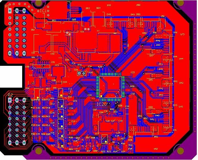
Depending on the function and design of electronic devices and equipment, printed circuit boards (PCBs) can be divided into single-sided, double-sided, and multi-layer boards according to the number of circuit layers. The number of multilayer boards can even reach more than a dozen layers. The emergence of High Density Interconnect (HDI) PCBs has promoted mobile phones, ultra-thin notebook computers, tablet computers, digital cameras, automotive electronics, digital cameras and other electronic products to reduce the motherboard design and achieve the goal of lightness, thinness and shortness., And more importantly, more internal space can be reserved for the battery, and the endurance of the device can be extended.
The biggest difference between HDI high-density interconnection technology and traditional printed circuit boards is the hole formation method. Traditional printed circuit boards use machine drilling methods, while HDI boards use non-machine drilling methods such as laser drilling. HDI boards are manufactured using the build-up method (Build Up). Generally, HDI boards basically use primary build-up, and high-end HDI boards use secondary or more build-up technology, and use electroplating to fill holes, stacked holes, and mine at the same time. Advanced PCB technology such as shot direct punching.
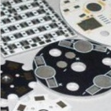
Mobile phone products vigorously use high-density connecting plates

The use of high-density interconnect boards has been very extensive. For example, the current built-in motherboards of smartphones are mainly HDI boards, and even any layer HDI (Any Layer HDI). The difference between the HDI process of any layer of high-density connection board and the general HDI is that the latter directly penetrates the PCB layer between the layers, while any layer of high-density connection board can omit the middle substrate, so that the thickness of the product can be changed. Get thinner. Generally speaking, the first-order HDI is changed to Any-layer HDI, which can reduce the volume by about 40%.
Apple and non-Apple products have adopted a large number of high-density connection boards of any layer. The main appeal is to make the product itself lighter and thinner, and to give the limited internal space to the battery to improve battery life.
Due to clear business opportunities, automation and PCB equipment factories continue to promote equipment technology to grasp huge business opportunities. Among them, the direct imaging exposure machine production technology introduced by Chuanbao Technology from the United States has been transferred to Taiwan for production. Chuanbao Technology originally cooperated with Maskless Lithography of the US, and obtained its technology transfer and patent authorization method, and introduced its direct imaging exposure machine to Taiwan for local production.
With regard to the current high-end thin-board and thin-circuit PCB production, it is an inevitable trend for the exposure process to abandon the film exposure and move towards direct imaging. In addition, Guangyun Machinery cut into high-end Any Layer HDI process PCB equipment in a project way.
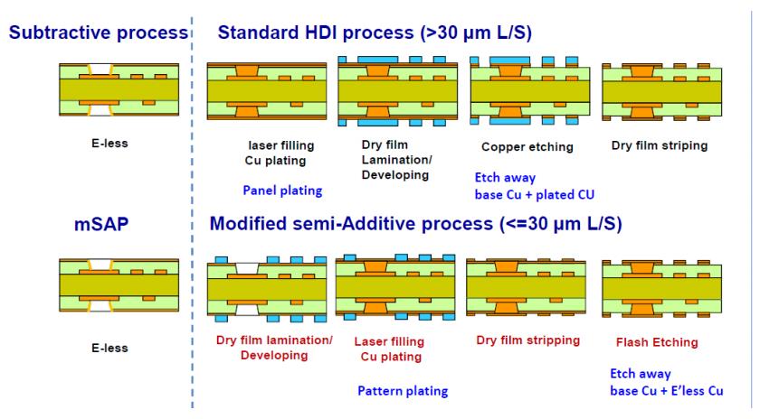
Introduction of substrate-like HDI technology using IC substrates
In order to cooperate with SiP technology, the line spacing and line width of HDI-like substrates will develop in the direction of fine pitch, especially the line spacing and line width must be reduced to less than 35 microns. This is the biggest difference from HDI boards. . Also because of the extreme shrinkage of the line spacing and line width, the traditional HDI process of printed circuit boards is no longer sufficient, and the HDI-like substrate must be produced by the semiconductor IC substrate process.
3D printing multilayer board has been realized
Printed circuit board manufacturing technology is changing with each passing day. It is worth mentioning that it is not uncommon to use 3D machines to print simple printed circuit boards. However, in the SolidWorks World 2016 conference, Nano Dimension in Israel used special nano-level conductive materials to It has even developed the world's first 3D printer DragonFly 2020 that can print professional multi-layer circuit boards.
Simon Fried, co-founder of Nano Dimension, said that this is the world’s first 3D printer that can print multi-layer circuit boards. It can support the through hole design of circuit boards. Printed circuit board materials, and the finished circuit board can also be welded with electronic components like ordinary circuit boards. This machine can print 4 layers or even up to 10 layers of circuit boards in a few hours.
Simon Fried also pointed out that the important key to printing multi-layer circuit boards is Nano Dimension’s exclusive nano-level silver conductive material AgCite, which can eject very fine silver ink droplets to print flat and three-dimensional electronic circuits. DragonFly 2020 uses inkjet technology and is equipped with two nozzles. By spraying conductive and insulating materials, they are printed layer by layer in a stacking manner to print multilayer circuit boards containing plane and three-dimensional circuits. However, the current Nano Dimension printing technology can only reach 90 Micron line width and the cost of silver conductive material is relatively high, so it is only suitable for circuit board proofing and small-volume production.
Complex lines increase the difficulty of verification
HDI boards are not the same as traditional multi-layer boards, so the testing and verification requirements for various properties are also different. As far as HDI boards are concerned, as HDI boards are getting thinner and thinner, coupled with the development of lead-free, the heat resistance is also more challenging, and the reliability of HDI has higher and higher requirements for heat resistance.
Heat resistance refers to the ability of PCB to resist thermo-mechanical stress generated during soldering. It is worth noting that the layer structure of HDI board is different from ordinary multi-layer through-hole PCB board, so the heat resistance of HDI board is the same as that of ordinary multi-layer Compared with the through-hole PCB board, the heat resistance defects of the first-order HDI board are mainly the board burst and delamination, and the area with the highest probability of the HDI board is the area above the dense buried holes and the area below the large copper surface., This is the focus of HDI testing.
On the whole, including HDI, the circuits of multi-layer boards are becoming more and more complex, and the size of circuit substrates is getting smaller and smaller, resulting in increasing process complexity and greatly increasing the difficulty of finished product verification. Therefore, it must be matched with high-end The test equipment conducts various electrical tests to avoid problematic substrates and improve the quality of PCB product manufacturing.