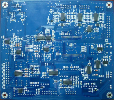
Reasonable layout of components in PCB design
Paying attention to the trend of environmental informationization and the development of various environmental protection technologies, PCB factory can start with big data to monitor corporate pollution and governance results, and find and solve environmental pollution problems in a timely manner. Keep up with the production concept of the new era, continuously improve resource utilization, and realize green production. Efforts to enable the PCB factory industry to achieve an efficient, economical and environmentally friendly production model, and actively respond to the country's environmental protection policy.
1. The beauty should not only consider the neat and orderly placement of components, but also the graceful and smooth wiring.
Because ordinary laymen sometimes emphasize the former more in order to one-sidedly evaluate the pros and cons of the circuit design, for the image of the product, the former should be given priority when the performance requirements are not harsh. However, in high-performance occasions, if you have to use double-sided boards and are also encapsulated in them and are usually invisible, you should prioritize the aesthetics of the wiring.
2. The stressed circuit board should be able to withstand various external forces and vibrations during installation and work.
For this reason, the circuit board should have a reasonable shape, and the positions of the various holes (screw holes, special-shaped holes) on the board should be arranged reasonably. Generally, the distance between the hole and the edge of the board should be at least greater than the diameter of the hole. At the same time, it should be noted that the weakest section of the plate caused by the special-shaped hole should also have sufficient bending strength. The connectors that directly "extend" from the device shell on the board must be reasonably fixed to ensure long-term reliability.

3. Heated For high-power, severely heating devices, in addition to ensuring heat dissipation conditions, they must also be placed in an appropriate location.
Especially in sophisticated analog systems, special attention should be paid to the adverse effects of the temperature field generated by these devices on the fragile preamplifier circuit. Generally, the part with very high power should be made into a module separately, and certain thermal isolation measures should be taken between it and the signal processing circuit.
4, signal interference is the most important factor to be considered in PCB layout design.
The most basic aspects are: the weak signal circuit is separated or even isolated from the strong signal circuit; the AC part is separated from the DC part; the high frequency part is separated from the low frequency part; pay attention to the direction of the signal line; the layout of the ground line; proper shielding and filtering And other measures. These have been repeatedly emphasized in a large number of treatises, so I won't repeat them here.
5. Installation refers to the specific application situation, in order to smoothly install the circuit board into the chassis, shell, slot, avoid space interference, short circuit and other accidents, and make the designated connector in the designated position on the chassis or shell. A series of basic requirements. Paying attention to the trend of environmental informationization and the development of various environmental protection technologies, PCB factories can start with big data to monitor corporate pollution and governance results, and find and solve environmental pollution problems in a timely manner. Keep up with the production concept of the new era, continuously improve resource utilization, and realize green production. Efforts to enable the PCB factory industry to achieve an efficient, economical and environmentally friendly production model, and actively respond to the country's environmental protection policy.