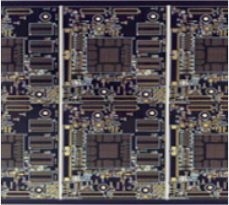
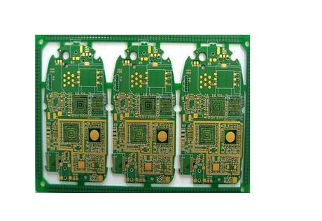
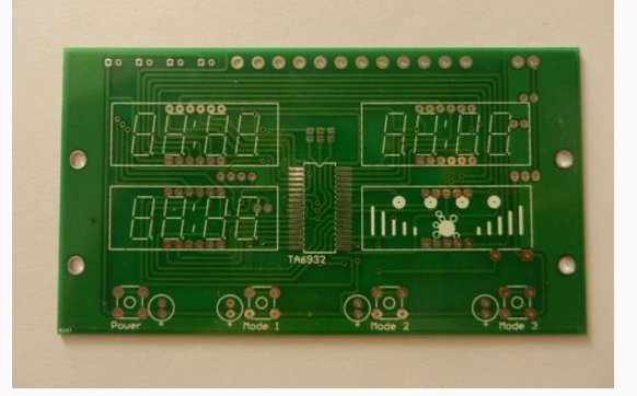
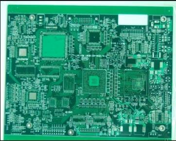
Circuit boards have become an important part of today’s electronic products. With the development of electronic technology and printed circuit board manufacturing technology, modern electronic products have become increasingly complex, and the density of printed circuit boards has increased. Testing and repairing are also becoming more difficult. In order to improve the degree of automation of the detection and maintenance of printed circuit boards, it is very necessary to design an automatic test system for circuit boards.
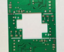
The following is an introduction to the inspection steps and precautions of PCB electroplating test boards
first step:
Check the various sections of the biopsy report according to customer requirements and company standards;
The second step:
Find the thickest and thinnest board in the test board, check the maximum and minimum aperture of each type of PTH aperture, and fill in the FA test board report;
third step:
Check the appearance of the test board;
the fourth step:
Check the etching report;

the fifth step:
After all the above items are qualified, confirm the plating instructions and notify the document control room to go online.
Precautions for PCB plating test board inspection:
The first point:
To judge whether the electroplating test board is qualified, it is necessary to synthesize the section report of the test room, the etching report of the production department and the actual measured aperture. The selection of the location of the FA slice should include the location of the large copper surface (or the location of dense lines), the isolated location and the location specified by the customer. It is required that the above three aspects can meet the second point of the requirement:
To judge whether the coating is qualified, it must be judged according to the standard. In addition to seeing whether it meets the minimum thickness requirements, it must be controlled not to be too thick.
The third point:
If the plating layer is too thick in individual isolated locations or the plating layer is too thin in individual lines (such as large copper surfaces), it is acceptable if it can meet the aperture requirements.
fourth point:
The standard for determining whether the electroplating layer is qualified: Generally speaking, for the finished hole wall copper thickness of 20μm, the copper thickness of the copper plating layer for one thickening is best to be 18~23μm. It is not allowed to exceed the lower limit, and two slices are allowed to exceed the upper limit but not More than 30μm. When the copper thickness of the finished hole wall is 25μm, the one-time thickening of the copper electroplating layer is controlled at 23~28μm, and the lower limit is not allowed. Two slices are allowed to exceed the upper limit, but it is not allowed to exceed 35μm. When the customer does not have the upper limit requirement for the coating, the upper limit can be appropriately relaxed on the basis of meeting the aperture and etching requirements.
Fifth:
For the same kind of hole, the largest hole will appear on the thinnest plate and the densest part of the board. On the contrary, the smallest hole will appear on the isolated position of the thickest plate. The above hole diameters should meet the requirements.
Sixth point:
Attention should be paid to distinguishing whether the copper thickening process is a primary thickening copper or a secondary thickening copper, so that the electroplated copper layer matches it, that is, the acceptance standard for the thickness of the secondary thickened copper electroplating copper layer should be reduced by 4μm.
Seventh point:
It is necessary to check the etched board for residual copper, short circuit or other abnormal phenomena, and find out the reason.
Eighth point:
For boards that fail to meet customer requirements for multiple test boards, it is necessary to find out the reasons and propose improvement measures to avoid similar problems in mass PCB production