The gigabit serial I/O technology has extremely outstanding superior performance, but these superior performance need conditions to guarantee, namely excellent signal integrity. For example, a supplier reported that when they first tried to use a high-speed, gigabit serial design for a specific application, the failure rate was 90%. In order to improve the success rate, we may need to perform simulations and adopt more complex new bypass circuits.
The GTP performance of Spartan-6 FPGA depends on the signal integrity of the PCB. The following factors need to be considered in the PCB design process: the laminated structure of the board, the layout of the components, and the signal routing.

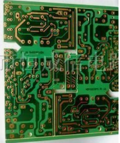
Power supply and stackup
For the GTP transceiver of Spartan-6 FPGA, the stack can be divided into two groups, the power distribution layer and the signal routing layer. The power layer is used to connect the MGTACC, MGTAVCCPLL, MGTAVTTTX and MGTAVTTRX power pins of GTP.
In the stack, the ground plane layer transmission signal line provides a signal return path. At the same time, because there is a shielded plane between the two signal layers, it is not necessary to consider the issues that need to be considered for the wiring of adjacent layers when the signal is routed, and more signal paths are provided.
The power plane of GTP should be closely adjacent to the ground plane to increase the coupling effect. The ground plane can provide shielding for the power plane of GTP, and shield the power plane from noise interference caused by the signal of the upper layer or the next layer.
In fact, consider from another perspective, that is, when the noise of the power supply appears in the high-frequency range, as the frequency increases, it becomes more and more difficult to find a capacitor that can cover this frequency range and achieve a filtering effect until it is impossible to find such a capacitor. . With the decrease of the capacitance value, the related stray inductance and the resistance value of the package do not change accordingly, so the frequency response will not change much. In order to achieve better power distribution at high speeds, we need to use the power layer and ground layer to construct our own capacitors. In order to achieve our goals more effectively, it is usually necessary to use adjacent power planes and ground planes.
The connection between GTP's power supply pins and the power distribution network plays a key role in the performance of GTP. PDN, and FPGA need low-impedance and low-noise connections. The FPGA's GTP power supply can tolerate a maximum noise of 10mVpp. In the range of 10KHz to 80MHz, the power supply can use a small plane. This small power plane should not cover the area of the SelectIO interface.
PCB design capacitor placement
In addition to considering the value of the bypass capacitor, another important aspect that needs to be considered is the placement of the capacitor.
The general rule is that the larger the capacitance, the less stringent the placement requirements. If the capacitor value is small, the capacitor should be as close as possible to the power and ground pins. One method that can be used is to remove the traces and vias of the unused general-purpose IO to make room for the bypass capacitor
The location of the GTP power segmentation area and the location of the GTP filter capacitor.
Signal routing
GTP signal traces and SelectIO signal traces should be avoided on adjacent layers, and their respective return paths should also be kept separate, including vias. It is important to maintain a certain distance between differential line pairs and between differential lines and other lines. The general rule is: the distance between adjacent line pairs must be at least 5 times the distance between the two lines in the line pair.
Gigabit signal differential lines should avoid changing the wiring layer as much as possible. If cross-layer transmission is necessary, you need to be especially careful. First, a complete return path must be provided. So we must couple the reference layer of layer A and the reference layer of layer B together. The most ideal situation is that both reference layers are strata. In this case, the return path can be achieved by placing another via connecting the two reference layers near the transfer layer via. If the reference planes are different (one is the ground plane and the other is the power plane), you need to place a 0.01μF capacitor as close as possible to the via to connect the two reference planes to reduce the impedance of the return path. Many problems may be encountered in the PCB design process, but as long as every detail is carefully done, a good PCB schematic can be designed.