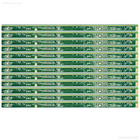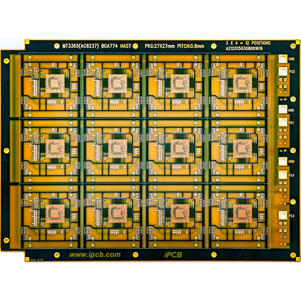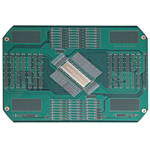


Model: Heavy Copper PCB
PCB Material: SY S1141
PCB Layer: 6Layers
Soldermask Color: Green
Silk Screen: White
Copper thickness: 2OZ/6OZ(70um)
Board Thickness: 2.8mmmm
Surface technology: Immersion Gold(1-3U)
Application: Power converter Heavy Copper PCB
Heavy Copper PCB is applied to components with strong current connection, transmission and hybrid connection. With the rapid development of automotive electronics and power communication modules, it has gradually become a kind of Havy Copper PCB with broad market prospects. According to market understanding, there is a demand for Heavy Copper PCB in automotive electronics, IGBT mounting, wind power converter, ignition coil, etc. On the other hand, with the wide application of PCB in the electronic field, the function requirement of Heavy Copper PCB is higher and higher. PCB will not only provide necessary electrical connection and mechanical support for electronic components, but also gradually be given more additional functions, so it can integrate power supply, provide large current, Highly reliable Eavy Copper PCB has gradually become a new product for iPCB.
At present, iPCB is manufacturing of Heavy Copper PCB by means of multiple solder-resistant printing-assisted layers or by using extra thick copper foil after the electroplated deposited copper is gradually thickened. However, the copper thickness of the above processes can only reach 0.41 mm (12 oz) at present, and Havy Copper PCB over 0.41 mm (12 oz) will become very difficult. IPCB has studied a new process method for manufacturing Heavy Copper PCB. Referring to the production technology of stacked master row, the Heavy Copper PCB with 0.5 mm (14 oz) or more has been manufactured by using embedded bonding technology of copper plate and process optimization.
Power converter Heavy Copper PCB is generally more than four layers of PCB, and the copper thickness is usually 1.6mm. The main reason is that the power converter Heavy Copper PCB has a large current and a high voltage, so the thin PCB cannot stand. Because the power converter Heavy Copper PCB is a high voltage power supply board, although it is made of copper, there are also some differences in the grade. Normal PCB materials are below normal TG140, power converter Heavy Copper PCB materials are generally above medium TG150, and high TG is 170. The higher the grade of PCB material, the better the temperature resistance and the higher the quality of the board.
However, the power converter Heavy Copper PCB itself has a high current and high voltage, so the design of the PCB is particularly important, considering not only the current but also the required voltage to pass through. An unreasonable design may cause the PCB to burn out. Some customers implement IPC-III standard and zero defect acceptance standard, which is much stricter than the general consumer PCB.

In standard FR-4 PCB, the minimum linewidth/spacing of iPCB inner 2OZ is 6/6mil

In standard FR-4 PCB, the minimum linewidth/spacing of the outer 2OZ of the iPCB is 7/7 mil
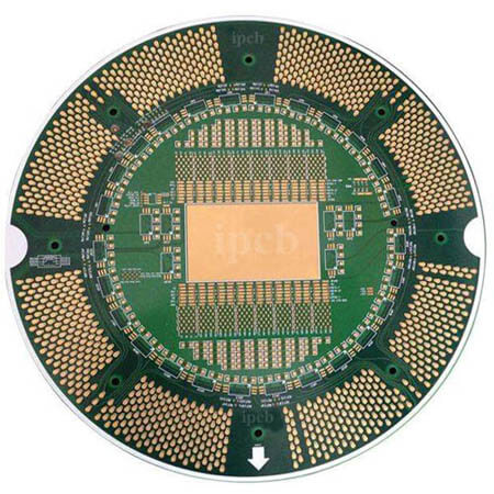
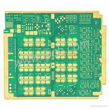
Manufacturing Process of Heavy Copper PCB
1. Laminated structure of Heavy Copper PCB
This is a Heavy Copper 4Layers PCB. The inner copper thickness is 2OZ, the outer copper thickness is 2OZ, and the outer minimum line width spacing is 0.3mm. The surface layer is FR4 copper clad (glass fibre epoxy resin clad), the total thickness of PCB is 1.6mm, the one-sided etching treatment, the bonding layer is non-fluidity PP sheet (semi-cured sheet), and the thickness is 0.1mm.
2. Processing method of Heavy Copper PCB
After overlaying and blackening treatment in Heavy Copper PCB, the blackening of copper plate can increase the surface area between the copper surface and the resin, and increase the wettability of the high temperature flowing resin to the copper, so that the resin can penetrate into the oxide layer gap, exhibit strong adhesion after hardening, and improve the bonding effect. At the same time, it can improve the laminable white spot phenomenon and the white and bubbles on the board caused by the baking test (287 [+] 6]). The specific blackening parameters are shown in Table 2.
The thickness of the inner Heavy Copper PCB and the FR-4 board used for peripheral filling can not be exactly the same because of the manufacturing error. If the conventional lamination method is used to bond, it is easy to produce defects such as laminated white spots and layers, which makes the bonding difficult. In order to reduce the bonding difficulty and ensure the dimension accuracy of the ultra-thick copper plate layer, through the test and verification, the monolithic bonding die structure is used, the top and bottom templates of the die are made of steel mould, and the silicone rubber pad is used as the intermediate buffer layer. By setting the appropriate parameters such as the lamination temperature, pressure and holding time, the lamination effect is achieved, and the technical problems such as white spots and layers of the ultra-thick copper layer are solved. Compression requirements of Heavy Copper PCB are met. Due to the low fluidity of non-fluidity PP resins, the use of normal covering material, kraft paper, can not make PP sheets uniformly compressed, resulting in defects such as white spots and layers after bonding. Silicone rubber pads are required as key buffer layers in the process of bonding for thick copper PCB products, which play a role in evenly distributing pressure during bonding. In addition, to solve the compression problem, the pressure parameter in the laminator is changed from 2.1 Mpa (22 kg/cm). ²) Adjust to 2.94 Mpa (30 kg/cm) ²), The temperature of PP sheet was adjusted to 170 C.
After testing according to chapter 4.8.5.8.2 of GJB362B-2009, PCB should be tested by 4.8.2 without more than 3.5.1.2.3 (subsurface defect) allowed bubbles and layers. PCB specimens meet 3.5.1 appearance and size requirements, are microdissected and examined by 4.8.3 to meet 3.5.2 requirements. In terms of lamination slicing conditions, the lines are full and seamless.
3. Heavy Copper PCB pressure test
The voltage resistance of each electrode in the Heavy Copper PCB sample was tested at AC1000V, without striking or flashing for 1 minute.
4. Heavy Copper PCB Large Current Temperature Rise Test
Designing the corresponding connecting copper plates to connect the poles in the Heavy Copper PCB sample in series, connect them to the large current generator and test them separately according to the corresponding test current. The high current temperature rise of ultra-thick copper PCB is related to its structure, and the temperature rise of different thick copper structures will be different.
5. Thermal stress test of Heavy Copper PCB
Thermal stress test requirements: After thermal stress test is carried out on the sample according to GJB362B-2009 general specification for rigid printed boards, no defects such as layering, foaming, warping of weld pad, white spot, etc. The Heavy Copper PCB sample should be micro-cut after its appearance and size meet the requirements. Because the inner layer of the sample is too thick to be metallographically cut, the sample is 287 (+) 6 (+) C After the thermal stress test, only the visual inspection of its appearance is performed.
The results of Heavy Copper PCB are no layers, blisters, warping of the pad, white spots
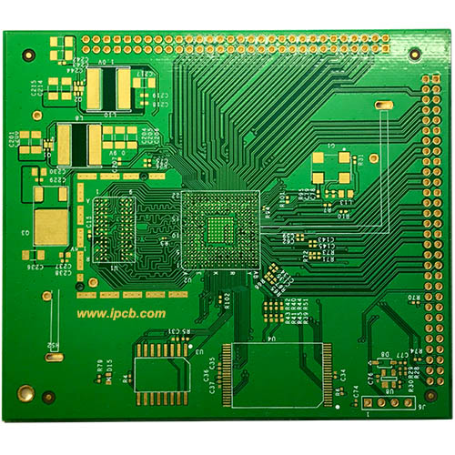
Model: Heavy Copper PCB
PCB Material: SY S1141
PCB Layer: 6Layers
Soldermask Color: Green
Silk Screen: White
Copper thickness: 2OZ/6OZ(70um)
Board Thickness: 2.8mmmm
Surface technology: Immersion Gold(1-3U)
Application: Power converter Heavy Copper PCB
For PCB technical problems, iPCB knowledgeable support team is here to help you with every step. You can also request PCB quotation here. Please contact E-mail sales@ipcb.com
We will respond very quickly.