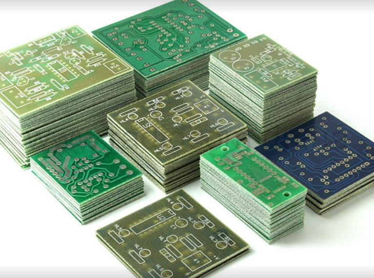
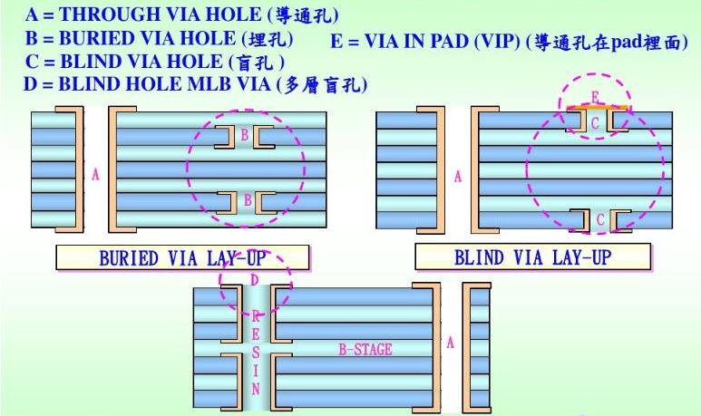
With the current design of portable products moving towards miniaturization and high density, PCB design is becoming more and more difficult, and higher requirements are put forward for the PCB production process. In most of the current portable products, the BGA package with a pitch of less than 0.65mm uses the design process of blind and buried vias. So what is the blind and buried via?
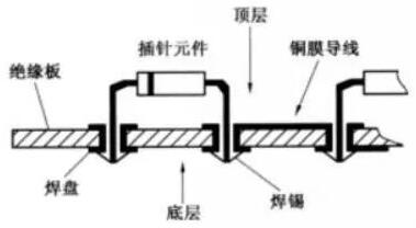
Blind vias (Blind vias / Laser Vias): Blind vias are vias that connect the inner traces of the PCB to the traces on the surface of the PCB. This hole does not penetrate the entire board.
Buried vias: Buried vias are the type of vias that only connect the traces between the inner layers, so they are invisible from the surface of the PCB.
An 8-layer board:
A: Through hole (L1-L8)
B: Buried hole (L2-L7)
C: Blind hole (L7-L8)
D: Blind hole (L1-L3)
2 Setting of blind and buried vias
Set Via type:
Click Setup-Pad Stacks in the menu, and then select Via option in Pad Stack Type, the settings dialog box as shown on the right will appear.
Click the Add Via button at the bottom left to set the Via type you need, including its drilling size, outer diameter size of each layer and other parameters.
If it is a through hole type, select Through in the Vias option at the bottom left, if it is a blind buried via type, select the Partial option
When selecting a Partial type via, you must specify its Start Layer and End Layer. For example, the blind and buried vias of the V12 and V27 types are set as shown in the figure below

3 PCB circuit board manufacturing process: blind and buried vias
When it comes to blind/buried vias, we start with traditional multilayer boards. The structure of the standard multi-layer board contains inner and outer circuits. Drilling holes and the metallization process in the holes are used to achieve the internal connection function of each layer of circuits. However, because of the increase in circuit density, the packaging methods of parts are constantly updated.
In order to allow the limited PCB area to place more high-performance parts, in addition to the thinner circuit width, the aperture is also reduced from 1 mm in the DIP jack aperture to 0.6 mm in the SMD, and further reduced to 0.4mm or less. But it still occupies the surface area, so there are buried holes and blind holes, which are defined as follows:
A. Buried Via
The through holes between the inner layers cannot be seen after pressing, so there is no need to occupy the area of the outer layer
B. Blind Via
Applied to the connection between the surface layer and one or more inner layers.
1. Buried hole design and production
The production process of buried vias is more complicated than that of traditional multilayer boards, and the cost is higher. Buried vias and general through holes and PAD size are generally specified.
2. Blind hole design and production
The board with extremely high density, double-sided SMD design, will have the outer layer up and down, and the I/O vias will interfere with each other, especially when there is a VIP (Via-in-pad) design, it is even more troublesome. Blind holes can solve this problem.