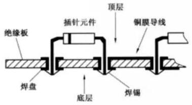
The PCB dimension of the drillings specified by the designer represent the final dimension from a manufacturers point of view. Due to the through-plating, the PCB surface finish and the copper build-up in particular, the drilling diameter has to be carried out larger to eventually reach the desired size. Plated-through drillings without an annular ring provide significantly less stability to the final PCB product.

The PCB drill-hole allowances for the fabrication of printed circuit board(PCB) may vary among manufacturers. In the PCB outer layers, an allowance of 0.3 mm for drill pads (plus the final diameter) by default is considered as sufficient. For a low-cost PCB mass production even larger allowances may be required.
Examples for drill allowances in the fabrication of printed circuit board(PCB):
Surface finish chemical gold:drill allowance +0.10 mm to +0.20 mm
Surface finish chemical tin:drill allowance +0.10 mm to +0.20 mm
Surface finish HAL (non-leaded):drill allowance +0.15 mm to +0.25 mm
If an allowance of 0.15 mm is applied, the annular rings width is 0.075 mm only (standard width: 0.3 mm plus the diameter of the PCBdrill-hole).
Desired size: 0.3 mm final diameter / 0.6 mm pad = 0.15 mm annular ring
Fabricated size: 0.45 mm drilling diameter / 0.6 mm pad = 0.075 mm annular ring
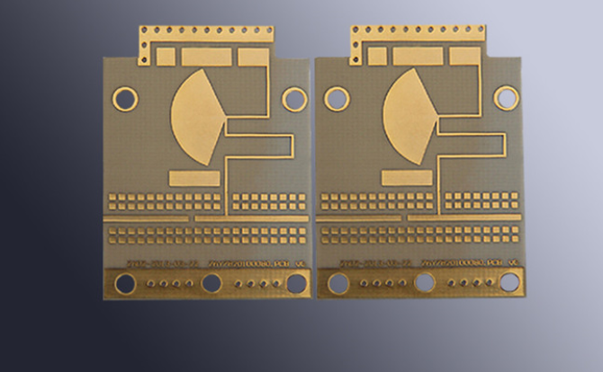
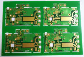
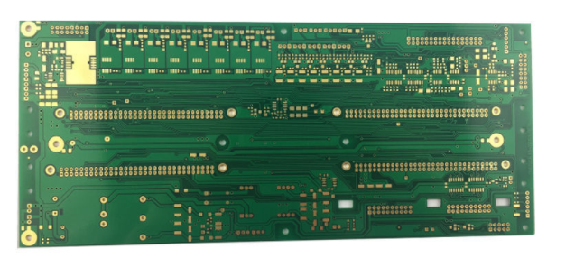
iPCB Circuit Co., Ltd. (iPCB®) is a High-Tech Manufacturing Enterprises focusing on the development and production of high precision PCB. Committed to domestic and oversea technology Enterprises to continue to provide the most cutting-edge, the most sophisticated PCB manufacturing services. The factory has an area of 23,000 square meters and 280 employees, among which the ratio of professional and technical personnel is more than 35%, and the personnel with bachelor degree or above accounts for 20%. The company has established sales network in Taiwan, Hong Kong, South Korea and else country, with Technology, Quality and Service as the guide, to provide high quality PCB processing and manufacturing services for domestic and foreign customers.