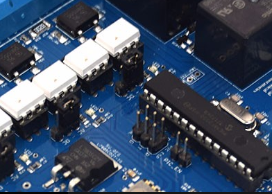
With the development of dedicated computing fields such as AI, 5G communications, and cloud computing, the computer architecture for the dedicated computing field has also entered a new golden age. Two important brushes depicting this golden age are open source hardware (chips) and agile development: open source can lower the threshold of chip design, and agile design can shorten the development cycle.
Speaking of open source chips, RISC-V can be said to be a representative of open source. Last year, the RISC-V International Foundation moved its headquarters to Switzerland. It currently has more than 1,000 members and approximately 200 corporate organizations. China occupies a very important role in this, Chinese companies account for more than 20%, and 9 of the 19 board members are from China.
As the open instruction set RISC-V is gradually sought after by the industry, the concept of open source chips has gradually entered people's field of vision, and has attracted worldwide attention and investment. Internationally, as early as the 2019 International Computer Architecture Flagship Conference ISCA's Vision Symposium, many American Academy of Engineering academicians including Turing Award winner Professor David Patterson, as well as from MIT, UC Berkeley, UCSD, Stanford, Google, Experts from top universities, enterprises and government agencies such as Nvidia and DARPA focused on the frontier hotspots of "agile open hardware for next-generation computing", involving content including instruction set, EDA tool chain open source, design process, high-level synthesis, Formal verification.
So what are the innovation opportunities for open source chips? Bao Yungang, deputy director of the Institute of Computing Technology of the Chinese Academy of Sciences, said at the technical forum: RISC-V belongs to the open instruction set. In fact, it is the open instruction set manual. For example, the instruction set manual of Intel CPU has more than 5000 pages, and the manual of ARM CPU The instruction set manual has more than 2,000 pages, while the RISC-V instruction set manual has only more than 200 pages. If the instruction set is turned into a real architecture, a lot of design documents will be generated at this time, then the documents can be made public; according to the design documents and then turned into source code, the source code can also be made public; the EDA tool chain can turn the open source code into a chip layout, Then EDA design tools can also be open source.

As we all know, the global EDA market is monopolized by the three major manufacturers Cadence, Synopsys, and Mentor (renamed as Siemens EDA in January 2021). Their large scale and complete product line can provide complete solutions for the entire process. On the contrary, domestic EDA tools have a market share of less than 5% in China and only 0.2% in the global market. Moreover, domestic EDA companies are small in scale, single in products, mostly "point" tools, and can only provide partial solutions. It is difficult for a single EDA tool to meet the designer's requirements for the entire process of IC design, and switching between different tools adds risks to data integrity. As a result, the market is increasingly calling for open source platforms.
Jie Biwei of Pengcheng Laboratory and the Institute of Computing Technology of the Chinese Academy of Sciences believes that open source EDA is an important guarantee for supporting the open chip ecology. Many successful experiences show that open source and openness are the necessary foundation for building a prosperous technological and industrial ecology. For example, the Linux operating system supports the entire open source ecosystem; another example is the Android mobile operating system. Although it is now closed source, it used open source as a starting point to unify the entire mobile Internet ecosystem except iOS; in the field of artificial intelligence, Caffe, TensorFlow, Pytorch, and PaddlePaddle can be said to be the cornerstones of the entire AI technology ecosystem.
Open source EDA tools can lower the threshold of chip design, such as reducing the cost of manpower, IP, and EDA for chip design. It can also provide good ideas for the development of basic scientific research and talent training in the field of EDA, whether it is for companies, universities, academic research institutions, or individual enthusiasts in the field of chips and EDA. If the open source EDA can gather multiple forces, it will help our country to accelerate to catch up with the international advanced level.
However, the foundation of my country's EDA software is still relatively weak, and it is almost blank in the open source field. Open source EDA still faces many challenges: few users, few contributors, and unclear framework structure; some solutions are also discussed on the forum. details as follows:
(1) Few users: The quality of open source EDA tools is far from commercial tools, and the number of users is very limited. The solution is to improve the quality of the tools and emphasize the project inspection in the production environment. That is, open source EDA tools should not only stay in academic papers and software codes, but must be combined with other point tools to form a tool chain to support complete chip tape-out verification and produce effective User feedback. For example, Magic in the United States has undergone several tape-out verifications, and the paper has actual chip test data.
(2) Few contributors: The EDA field is relatively niche, and its open source community is even thinner. The main contributors to open source tools such as Yosys, abc, magic, and OpenROAD are mostly about 10 people. Due to the characteristics of the EDA discipline, open source EDA contributors need to have knowledge of CS, Math, EE and MicroE at the same time, and the technical threshold is relatively high. The development of each open source EDA tool is not open. It is basically an internal team of a certain school, research institution, and company. There are few external participants and it is difficult to participate. The solution is to fully disassemble, abstract and describe EDA technical problems, and classify them into language expressions that can be understood in professional fields such as mathematics, algorithms and high performance, and mobilize community forces in multiple disciplines.
(3) Unclear framework structure: Inconsistent code and low reuse rate are a common problem of open source software. However, the strong binding of open source EDA tools and algorithms makes the problem more prominent. Designing new algorithms usually requires a lot of code rewriting, which loses the meaning of open source. There are two solutions. First, modular design, starting from the design of the basic framework, and then going to the algorithm layer, abstracting common operations and data formats, exploring iterative reconstruction rules from the code, and forming a streamlined, efficient and modular basic framework. This modular design also facilitates the acceleration of the EDA design process with a distributed parallel computing architecture. Second, standardize abstraction. Use excellent compiler design concepts such as MulTI-level Intermediate RepresentaTIon (MLIR) to divide the entire design process (especially front-end design) into multiple abstract levels, so that experts in various fields can focus on their respective abstract levels., At the same time, through the compilation of multiple levels to open up the EDA tool chain, complete agile and convenient full-process verification. In this way, even a point tool can be flexibly connected to the open source EDA tool chain through a standardized conversion format to fully verify the performance and quality of the tools developed by oneself. At present, North American industry and academia are forming this trend.
As far as the open source EDA project is concerned, no matter from low process (110nm) to high process (55nm, 40nm or even 28nm). From university teaching-level applications to enterprise product-level applications, from small-scale ASIC chips to larger-scale SoC projects, the strategy of combining research and application should be adhered to, with practicality as the driving force, and application of research and application of research to application. Break down one by one from five aspects: tool chain, point tool, benchmark test set, demonstration application, and industrial-grade open source process library.
Research progress in the industry
It is worth mentioning that at the ASPLOS 2021 conference, Dr. Chris Lattner (one of the main initiators and authors of the LLVM project and the author of the Clang compiler), who has just moved from Google Brain to the star RISC-V company SiFive, did The Golden Age of Compiler Design in an Era of HW/SW Co-design's speech, proposed a new unified EDA (Electronic Design AutomaTIon) framework based on MLIR compilation technology, and designed a tool chain for EDA like TensorFlow or PyTorch in software Provide a complete and flexible infrastructure. The CIRCT project is the same as MLIR, and it is easy to form ecological consistency in hardware design and software compilation.
On the road of open source EDA software, domestic EDA academics and industries are striving to find suitable positions to contribute to open source EDA.
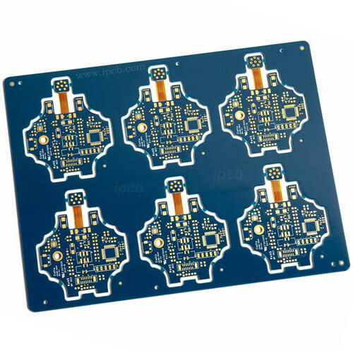
In the field of open source chips, the Institute of Computing Technology of the Chinese Academy of Sciences launched projects such as RISC-V processor chips and RISC-V native operating systems in 2019, and built an open source chip technology system with cost-effective advantages on the domestic 28nm process. In addition, they are also exploring open source EDA to design open source chips. Based on existing open source tools, they have built a Python-based RTL to GDS2 design process; in August last year, five undergraduates from National University of Science and Technology used open source EDA tools for two years. Designed the Guohu-1 chip and realized tape out.
The Chinese Academy of Sciences has also developed AgileServe, a cloud platform for chip agile design, which integrates various open source elements to support users to quickly customize processor chips and software development, and lower the threshold of chip design. For students, chip design can be carried out anytime and anywhere; for teachers, it is possible to guide students online.
Chen Gang, executive deputy general manager of Nanjing Integrated Circuit Design Service Industry Innovation Center Co., Ltd. (hereinafter referred to as EDA Innovation Center), introduced the use of open source methods to create a domestic EDA universal base (openEDI). Considering that the domestic EDA point tools are independent, and building a common base for the domestic ecology, it is expected that the point tools will be connected together. The research and development goal of the EDA universal base is to support all domestic EDA tools, aggregate a complete set of EDA tool chains, and become a domestic ecological universal base. The picture below shows the EDA general base architecture. The bottom part is the data layer, which carries all EDA databases and data models on memory and disk, including various parser modules, user interface modules, and so on. The upper layer is the general algorithm layer and calculation framework.
Lin Yibo of Peking University introduced the well-known "Deep Learning Assisted Place and Route Optimization" project at the meeting. He described the use of deep learning to improve traditional place and route algorithms. In this process, open source place and route tools must be used, otherwise it will be very difficult. Difficult to obtain deep learning samples. In the future, they will continue to improve the algorithm, increase stability and generalization ability. It is expected that an open EDA data set such as ImageNet may be released to attract the mutual competition and development of academia and industry.
Yan Hao of the National ASIC System Engineering Technology Research Center of Southeast University described the development of wide-voltage near-threshold design methodology and open source EDA. He introduced that the technical challenge of EDA tools is the development of deviation modeling and optimization algorithms brought by the evolving process and etching dimensions. He pointed out that when doing research, the biggest challenge is the need to spend a lot of energy to reproduce other people's code, so they also cooperate with domestic EDA companies such as NiiCEDA and actively invest in the development of open source timing analysis tools.
Zhu Zhufei from Ningbo University shared the research progress on multi-logic domain automatic synthesis tools. He said that logic synthesis is to convert all the RTL-level descriptions of digital circuits designed into the connections of the unit circuits in the specified process library under the condition of satisfying constraints. Logic synthesis mainly includes three stages: translation, optimization and process mapping. He pointed out that the comprehensive methods developed from different logical complete sets are applicable to different scenarios. The existing EDA tools are all developed based on traditional Boolean logic. New types of operators can bring more opportunities, such as polarity transformation. Reed-Muller, TB and RM dual logic, etc. In terms of EDA open source, he pointed out the development trend of logic synthesis tools: 1. AI for EDA, using AI methods to infer the order of logic synthesis optimization transformation, so that engineers without any experience can get an optimization script; 2. EDA for AI, use The logic operation is reversed in the form of a lookup table to achieve the same purpose as the training weight of the neural network; 3. Optimal Solution, given a digital circuit, the existing method highly depends on the SAT solver to obtain the minimum number of nodes, minimum logic depth, etc. Excellent solution, but the SAT solver itself is a heuristic algorithm, and digital circuit simulation can assist SAT to perform more efficient search; 4. Technology Enabler, develop new logical abstraction methods, and assist in the evaluation of new processes such as two-dimensional materials And development. Regardless of the training set, search optimization and new models will benefit from the open source ecosystem.
Where does the open source EDA go?
The open source EDA ecosystem faces many difficulties from 0 to 1. How to get through the closed loop of the open source EDA ecosystem? How to maintain the sustainable development of the ecology? How to prevent ecological risks such as tapeout failure, IP leakage, and patents? Where should we go in the future? Regarding these issues, the scholars and experts present had different opinions and conducted intense and meaningful discussions.
From 0 to 1, the ecology of open source EDA starts from the academic world
Unlike traditional open source software, the data structure, code quality, and algorithm of open source EDA software are extremely professional, and the user group is small, which limits the scale of the open source community. Throughout history, Silicon Valley's high-tech companies, as small as stars and seas, all started from university innovation. EDA is the same. First, cultivate the first group of users of open source EDA in colleges and universities, including teachers and students, let them use open source tools in innovative ways, and then through continuous use and iterative improvement of tools, they will be usable in the future. degree.
However, it is also challenging to promote and maintain the closed-loop EDA ecosystem from the academic world. The most important issue is the development of academia's participation in open source EDA and the continuous maintenance of open source projects. From a utilitarian point of view, when university researchers transfer their research interests or the end of the project, the motivation to maintain open source projects disappears; students spend years of experience learning and mastering open source EDA tools, it is better to master commercial tools that are more practical for job hunting; high quality There is not much open source work for students, and students reimplement an algorithm or tool sometimes faster than hacking (or even debugging) the code of an open source project. After students graduate, if there is no good documentation and high-quality code management, then the follow-up academic continued to iterative development motivation is not enough.
Therefore, the forum recommends that the academic evaluation standards of universities be properly guided, so that open source projects with high code and document quality, and projects with many stars on code hosting and collaboration platforms such as Github/Gitee become academic business cards for university scholars, students, and corporate experts. Starting and maintaining open source EDA projects will be a great incentive for students to get employed.
The establishment of an open source EDA ecosystem also requires a benchmark test set, especially an industrial benchmark test set that can complete an end-to-end process; how to go from a small-scale data set in academia to an industrial-level advanced design is a topic that needs to be discussed. Can well-known chip design companies in the industry provide some desensitized designs so that the open source community can use this as a reference for academic research and student competitions, so as to expand the scale of the open source community. In particular, in the contemporary era where deep learning technology is closely integrated with the EDA field, an "ImageNet" in the field of chip design is needed to promote community prosperity.