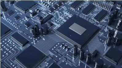
Multi-chip packaging (MCP) has long met the need to pack more performance and features into a smaller and smaller space(PCB). It is natural to expect the MCP of memory to be extended to include ASICs such as baseband or multimedia processors. But there are difficulties with this, namely high development costs and ownership/reduction costs. How to solve these problems? The concept of cascading IC Packaging (POP) is gaining wide acceptance in the industry.
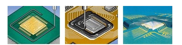
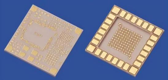
POP (Packaging on Packaging), also known as stack assembly, also known as Packaging layer. POP is a package consisting of two or more bgas (ball-grid array package) stacked on top of each other. In general, the stack package structure of POP adopts BGA solder ball structure, which integrates high-density digital or mixed signal logic devices at the bottom of the POP package to meet the characteristics of multi-pin logic devices. As a new type of highly integrated packaging form, POP is mainly used in modern smart phones, digital cameras and other portable electronic products, and plays a very wide role.

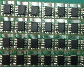
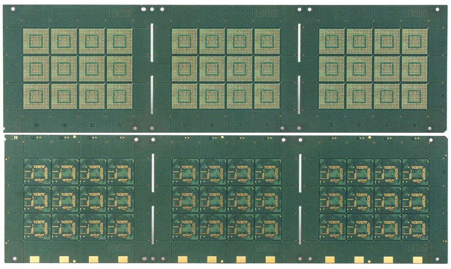
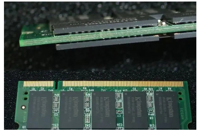
MCP is a hybrid technology that vertically stacks various types of memory or non-memory chips of different sizes in a plastic encapsulated case. It saves space on small printed circuit board PCB in this way.
From the perspective of architecture, SIP is to integrate multiple functional chips, including processor, memory and other functional chips into one package, so as to realize a basic complete function. From the point of view of terminal electronic products, SIP is not only concerned about the performance/power consumption of the chip itself, but also realizes the short, thin, multi-functional and low-power consumption of the entire terminal electronic products. After the rise of lightweight products such as mobile device and wearer-device, SIP demand is becoming increasingly apparent.
The basic concept of SoC is to integrate more devices on the same bare metal chip to achieve the goal of reducing size, enhancing performance and reducing cost. However, in the mobile phone market, where project lifecycles are very short and cost requirements are very demanding, SOC solutions have significant limitations. From a memory configuration point of view, different types of memory require a lot of logic, and mastering different design rules and techniques can be very challenging, affecting development time and the flexibility required by the application.
SOC and SIP
SOC is very similar to SIP in that both combine a system containing logical components, memory components, and even passive components into a single unit. From a design perspective, SOC is a high degree of integration of the components required by the system onto a chip. From the point of view of packaging, SIP is a side-by-side or superimposed packaging method for different chips. It is a single standard package that integrates multiple active electronic components with different functions, optional passive devices, and other devices such as MEMS or optical devices to achieve certain functions.
In terms of integration, in general, SoC only integrates logical systems such as AP, while SIP integrates AP+ MobiledDR. To some extent, SIP=SoC+DDR. With higher and higher integration in the future, EMMC is likely to be integrated into SIP. From the perspective of packaging development, SOC has been established as the key and development direction of future electronic product design due to the requirements of electronic products in terms of volume, processing speed or electrical characteristics. However, with the increasing cost of SOC production and frequent technical obstacles in recent years, the development of SOC is faced with bottlenecks, thus making the development of SIP more and more attention by the industry.

Development path from MCP to POP
Combo(Flash+RAM) memory products that integrate multiple FLASH NOR, NAND, and RAM in a single package are widely used in mobile phone applications. These single-package solutions include multi chip package (MCP), system-level package (SIP), and multi chip module (MCM).
The need to provide more functionality in increasingly small mobile phones is a major driver of MCP's growth, however, developing solutions that enhance performance while maintaining a small size is a formidable challenge. Not only size is an issue, but performance is also an issue, such as the use of MCP memory with SDRAM and DDR interfaces when working with baseband chipsets or multimedia coprocessors in mobile phones.
POP stack packaging is a good way to achieve miniaturization with a high degree of integration. In stack packaging, out-of-package (POP) is becoming increasingly important in the packaging industry, especially in mobile applications, because of its ability to stack logical units with high density.
Advantages of POP encapsulation
1.storage devices and logic devices can be tested or replaced separately, to ensure the yield;
2.Double layer POP package saves the substrate area, and the larger longitudinal space allows more layers of packaging;
3.Mixed DRAM, DDRAMSRAM, FLASH, and microprocessor along the longitudinal PCB;
4.For different manufacturers of chips, provide design flexibility, can be simply mixed together to meet customer needs, reduce the complexity and cost of design;
5.At present, the technology can be used to overlay and assemble the layer chip in the vertical direction;
6.The electrical connection of the top and bottom devices stacked together realizes faster data transmission rate and can cope with the high-speed interconnection between logic devices and storage devices