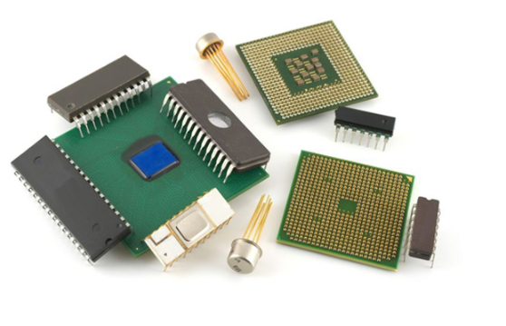
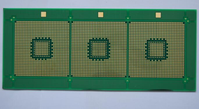
In the past hundred years, with the rapid development of integrated circuit, IC packaging board technology has also been improved, THE application demand of IC industry is getting bigger and bigger, the integration is getting higher and higher. The general development process of packaging: TO-DIP-PLCC-QFP-PGA-BGA-CSP-MCM, the technical indicators are advanced generation by generation, the chip area and package area ratio is closer and closer TO 1, electrical performance and reliability gradually improve, the volume is smaller and thinner.
1.MCM (multi-chip component)
In fact, it's a chip component, the latest technology. It is a packaging technology that assembles multiple semiconductor bare chips on a wiring substrate. Therefore, it eliminates IC packaging materials and processes, thus saving materials. , while reducing the necessary manufacturing process, so strictly speaking the product is high-density assembly
Open Tencent News to see more pictures
2. CSP (chip-level package)
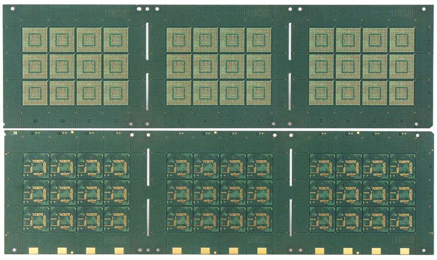
CSP package is chip level package. As we all know, chips are essentially small. Therefore, CSP package of the latest generation of memory chip packaging technology can make the chip area to package area ratio of more than 1:1.14, quite close. The ideal situation of 1:1 is rated by the industry as the highest form of single chip. Compared to THE BGA package board, the CSP package can increase the storage capacity by three times in the same space. This package is characterized by small size, a large number of input/output terminals, and good electrical performance. There are CSP BGA (ball grid array), LFCSP (lead frame), LGA (grid array), WLCSP (wafer level) and so on.
1.CSP BGA

2. LFCSP (lead structure)
LFCSP, this package is similar to the lead frame that uses conventional plastic packaging circuits, but is smaller in size and thinner in thickness, with finger pads extending into the inner area of the chip. The LFCSP is a plastic package based on a lead frame. The internal interconnection of the package is usually achieved by wiring, and the external electrical connection is achieved by welding the peripheral pins to the PCB board. In addition to pins, LFCSPS typically have larger exposed heat pads that can be welded to the PCB to improve heat dissipation.
3. LGA (Grid Array)
This is a grid-array package, similar to BGA, except that BGA is soldered, while LGA can be unlocked and replaced at any time. That is, it is replaceable compared to the BGA, but the replacement process needs to be very careful.
4. WLCSP (wafer level)

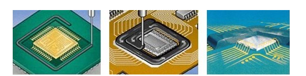
4. BGA (Ball grid Array)
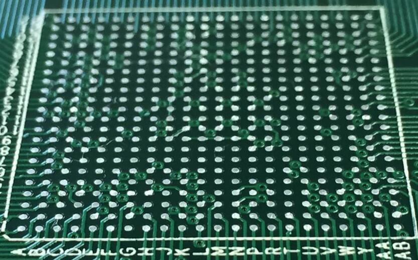
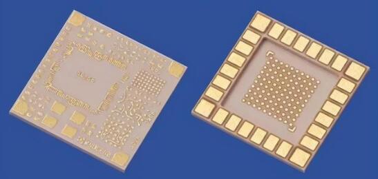
One of the ball contact arrays, surface mount packages. On the back of the PCB, spherical bulks are made in display mode in place of pins, and the LSI chip is assembled on the front of the PCB, which is then sealed with molded resin or potting. Also known as bump display carrier (PAC). BGA mainly includes: PBGA (plastic package BGA), CBGA (ceramic package BGA), CCBGA (ceramic cylinder package BGA), TBGA (carrier package BGA) and so on. Currently used BGA packaging devices, according to the substrate type, mainly include CBGA (ceramic grid array package), PBGA (plastic grid array package), TBGA (carrier grid array package), FC-BGA (flip-chip grid array package), EPBG (enhanced plastic grid array package), etc.
4-1 CBGA (ceramics)

CBGA has the longest history in the BGA package family. The base plate is multi-layer ceramic, and the metal cover plate is welded on the base plate with sealing solder to protect the chip, lead and pad. This is a surface mount package with a set of solders at the bottom for easy access.
4-2FCBGA

FCBGA realizes direct connection between chip solder ball and BGA substrate by flip chip. In BGA products, higher package density can be achieved and better electrical and thermal performance can be obtained.
4-3PBGA

BGA package, it uses BT resin/glass laminate as the substrate, plastic epoxy molding plastic as the sealing material. This kind of encapsulation chip is sensitive to moisture and is not suitable for device encapsulation with high requirements on air tightness and reliability.
4-4 SBGA

SBGA uses an advanced substrate design, including copper fins for enhanced heat dissipation, while using reliable assembly processes and materials to ensure high reliability and superior performance. Combining high performance with light weight, a typical 35mm² SBGA package mounts to a height of less than 1.4mm and weighs just 7.09.
5.PGA (Needle Grid Array)

Display pin encapsulation. In one plug-in package, the vertical pins on the bottom are arranged in an array. The packaging substrate is basically a multilayer ceramic substrate. Used for high-speed large-scale logical LSI circuits. Pins are at the bottom of the chip, typically square, and the distance from the center to the pin is generally 2.54mm. The number of pins varies from 64 to 447. There are generally two types: CPGA (Ceramic Pin Grid Array Package) and PPGA (plastic Pin Grid Array Package).
6. QFP (Quad Flat Package)
This type of package is a square flat package, usually square, with four sides of the pins. This package implements the CPU chip pin spacing is very small, pin is very thin. Generally large scale or very large scale integrated circuit adopts this package, the number of pins is generally more than 100. Due to its smaller package size, parasitic parameters are reduced, suitable for high frequency applications. Such packages are: In this process, CQFP (Ceramic Quad Flat Package), PQFP (Plastic Quad Flat Package), SSQFP (Self Binder Quad Flat Package), TQFP (Slim Quad) Flat Package), SQFP (Shrink Quad Flat Package)
1. LQFP (thin)
This is a thin QFP. Refers to the QFP with a package thickness of 1.4mm, which is the name used by the Japanese electronic machinery industry according to the newly developed QFP shape specification.
2. TQFP (Thin Square)
7. LCC (lead or lead-free chip carrier)
A ceramic chip carrier with pins, one of a surface-mount package, with pins leading from the four sides of the package. It is a package for high speed hf IC, also known as ceramic QFN or QFN-C.
1. CLCC (wing pin)
2. Least developed countries
C-shaped pin chip carrier, the pin is pulled out from the top of the chip and bent down into a C-shaped shape
3.PLCC
The pins are drawn from the four sides of the package and are t-shaped and made of plastic. Pin center spacing was 1.27mm and pin number ranged from 18 to 84. It is easier to operate than QFP, but more difficult to inspect the appearance after welding.
8. SIP (single-in-line Encapsulation)
A single in-line package lead leads from one side of the package in a straight line. Usually a through-pass, the pins lead from one side of the package and are lined up in a straight line. When assembled on a printed circuit board, the package is side-standing. Pin center distance is usually 2.54mm, pin number varies from 2 to 23, most of which are customized products. The shapes of packages vary.
9. SOIC (small IC)
SOIC is a small shape integrated circuit package. The number of external leads shall not exceed 28 small shape ics. Generally, there are two types of encapsulation: wide body and narrow body. This is about 30-50% less space than the same DIP package. The thickness is reduced by about 70%.
10. SOP (small package)
SOP packaging is a form of component packaging. Common packaging materials are: plastic, ceramic, glass, metal, and so on, now the basic use of plastic packaging. It has a wide range of applications, mainly used in a variety of integrated circuits. Then came TSOP (thin small profile package), VSOP (very small profile package), SSOP (reduced profile package), TSSOP (thin reduced profile package), MSOP (microprofile package), QSOP (quarter size profile package), QVSOP (quarter size very small profile package), and others.
1. SSOP (reduced type)
2. TSOP (Thin small shape package)
3. TSSOP (Thin reduction)
11. SOT (Small transistor)
SOT is a type of SMD package. For devices with less than 5 pins (3pin, 4pin), the SMD package is usually adopted. Small size, many transistors are used in this package.
This is also a transistor package. Generally both sides have pins, the number of pins is 3, 4, 5, most not more than 7.
12. DIP (double wire package)
DIP packages are also known as dual - in - line packages or dual - in - line packages. Most small and medium-sized integrated circuits use this form of packaging, pin number is generally not more than 100. Chips in this package have two rows of leads. Pins can be welded directly to a DIP structure chip socket or to a weld position with the same number of holes. Its characteristic is can easily realize PCB board drilling welding, good compatibility with the motherboard.
1. CerDIP (Ceramic dual in-line Package)
Cerdip ceramic dual in-line package for ECL RAM, DSP (Digital Signal Processor) and other circuits. Cerdip with glass window is used for ULTRAVIOLET erasable EPROM and microcomputer circuits with built-in EPROM, etc.
2. PDIP (plastic package)
This kind of plastic double - in - line package is quite common. Suitable for PCB through hole installation. Simple operation, can use IC socket debugging. But the package size is much larger than the chip, packaging efficiency is very low. A lot of effective installation area.
13. TO (Transistor shape package)
IC packaging board TO is a transistor shape package. One is a transistor package type that allows the lead to be surface mount, and the other is a round metal case package with no surface mount components. This package is widely used, many transistors, MOS tubes, thyristors and so on are used this package.