The principle and application of 3D IC Packaging
The 2.5D mediating layer is a configuration in which the tube cores are installed side by side on a silicon, glass or organic mediating layer using a silicon through hole (TSV) through the mediating layer. (When glass or organic laminates are used as the substrate for the intermediate layer, they are called through glass through holes (TGV) and substrate through holes (TSV) respectively.) Communication between cores is carried out through a circuit manufactured on the intermediate layer.
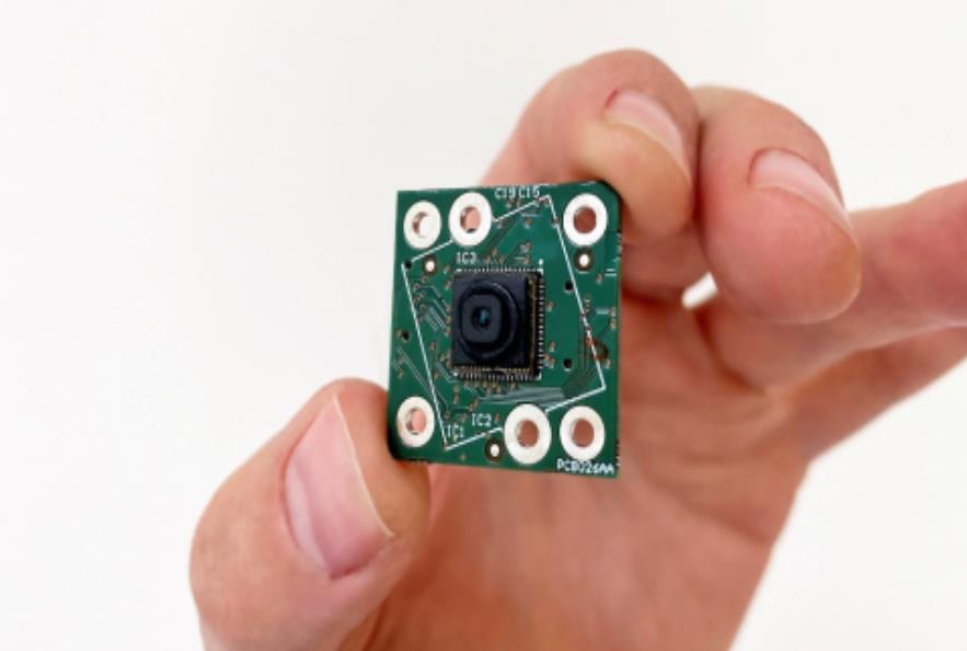
CMOS image sensors (CIS) have TSV as backside holes to form interconnects, eliminating lead key merges allowing for reduced size and increased density. In all types of 3D packages, the chips in the package use off-chip signals to communicate as if they were mounted in a separate package on a normal circuit board.
3D IC can be divided into 3D stacked IC (3D-sic), which means that the IC chip is stacked and interconnected with TSV; And true 3D ics, which use the FAB process to stack multiple device layers on a single chip, may or may not use very finely spaced TSVS to form interconnects.

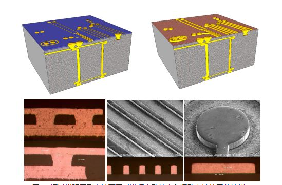
Silicon through holes (TSV) are holes created in silicon wafers using an etching process. The interconnection is formed by filling the TSV with a conductive material such as copper, tungsten or polysilicon (Figure 2). The main advantage of TSV interconnects is that they shorten the path through which signals travel from one chip to the next or from one layer of circuit to the next. This allows for reduced power and the ability to increase interconnection density, thus improving function and performance. The TSV itself is not a 3D IC. Instead, they are the basis for enabling 3D ics. Backside through holes are also used in other devices, such as image sensors, microelectromechanical systems (MEMS), and compound semiconductors.
What is the meaning of monolithic 3D IC?
Instead of stacking wafers or modules to create a 3D IC, a monolithic 3D IC starts with a base wafer on which additional layers such as crystalline silicon, metal layers, and active and passive circuits are added using traditional FAB devices (Figure 2). Vertical interconnects are formed between layers rather than between chips using through holes in the nanometer rather than the micron range; Same as TSV. Several different approaches are being developed, primarily for in-memory applications. Integral 3D is sometimes called sequential 3D.
What is 3D memory?
Many methods have been developed to stack memory perpendicular to two non-volatile (NAND flash) and volatile (DRAM) memory devices. DRAM methods include high bandwidth memory (HBM), Micron's mixed memory cube and Tezzaron's integrated RAM (DiRAM). All of this is based on a 3D IC using TSV (Figure 3). Samsung, Toshiba and many others are developing 3D NAND flash based on holistic 3D approaches.
What are the benefits of 2.5D inserter technology?
Originally developed as a bridging technology for 3D ics, 2.5D technology has grown into a packaging platform that is expected to coexist with 3D ics. Unlike 3D-IC, only the intermediary layer (not the core itself) requires the TSV to connect the active core to the package substrate. This allows the use of existing mold designs.
What are the main technical drivers of 3D integration?
The increased cost of this lithography step and wafer processing in general at the node of next-generation chips is driving the industry to look for alternatives to improve the performance and functionality of our electronic devices and reduce costs. In addition, the need to integrate various technologies (logic, memory, RF, sensors, etc.) at small sizes is driving the industry to embrace 3D integration as a solution.
What are the market drivers for 3D integration?
The market drive for 3D integration (3D integration) begins with high-end computing, servers and data centers, military and aerospace, and medical equipment, as they are in greatest demand and can afford the cost of current 3D integration technologies. Tablets, smartphones and gaming devices are also driving the technology.
What challenges do 3D ics face?
While many claim that there are no remaining technical challenges and that the remaining issues can be easily addressed, some process steps still require better solutions, such as design tools for planning, implementing and verifying 2.5D and 3D ics, wafer processing, thermal management and testing. The main challenges are current unit costs, low quantities and implementation risks due to the maturing of the ecosystem. Efforts are being made to reduce process costs and simplify collaboration across the industry. Increased production will help to reduce costs. However, many 3D experts believe that implementing 3D ics will greatly reduce system costs, and that the remaining challenge is to educate system-level engineers about the benefits of designing 3D ics in their systems.

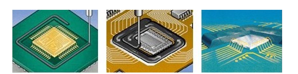
CMOS image sensor (CIS) is one of the first devices to implement through hole back through hole in large quantities. CIS with backside lighting (BSI) is now in production, and since the CIS is stacked on top of the IC, it is a 3D IC device (Figure 2). Xilinx introduced a 2.5D plug-in design for all programmable FPgas of its Virtex-7 series in 2011. Over the past few years, Tezzaron has delivered small quantities of DiRAM.
In late 2014, Micron and Samsung will begin production of hybrid storage Cubes (HMCS), which are 3D DRAM stacks on top of logic devices. SK Hynix will provide both HMC and HIGH bandwidth memory (HBM). Mass production of these 3D integrated storage devices took place in 2014/15 and continued to use logic stacks and heterogeneous devices for several years after that.
iPCB will share all the information with you!