This article uses simple mathematical formulas and electromagnetic theory to explain the hidden behavior and characteristics of passive components on PCB board. These are the basic knowledge that engineers must have in advance when designing electronic products to pass the EMC standard. . Traditionally, EMC has been regarded as black magic. In fact, EMC can be understood by mathematical formulas. However, even if mathematical analysis methods can be used, those mathematical formulas are still too much for actual EMC circuit design. Too complicated. Fortunately, in most practical work, engineers do not need to fully understand the complex mathematical formulas and the theoretical basis that exists in the EMC specification, as long as simple mathematical models are used, they can understand how to Meet EMC requirements.

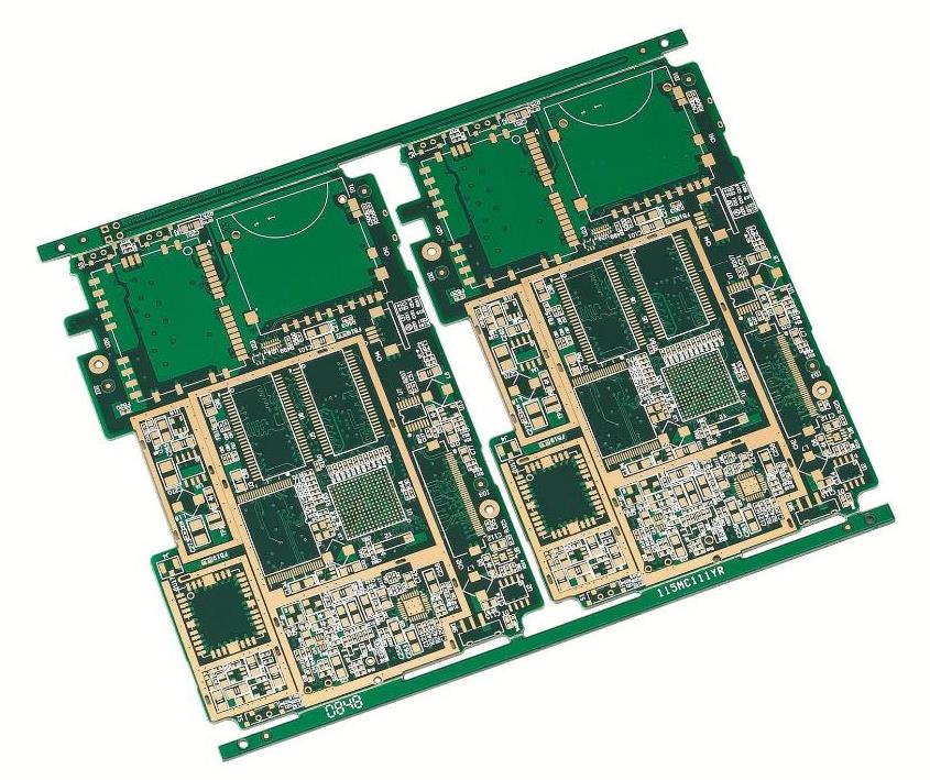
1. Wire and PCB board traces
Seemingly inconspicuous components such as wires, traces, fixtures, etc., often become transmitters of RF energy (ie, EMI). Every component has an inductor, which includes the bonding wires of the silicon chip, and the pins of the resistors, capacitors, and inductors. Every wire or trace contains hidden parasitic capacitance and inductance. These parasitic components affect the impedance of the wire and are sensitive to frequency. Depending on the value of LC (which determines the self-resonant frequency) and the length of the PCB trace, self-resonance can occur between a component and the PCB trace, thus forming an efficient radiating antenna. At low frequencies, the wire is roughly only resistive. But at high frequencies, the wire has the characteristics of inductance. Because after becoming high frequency, it will cause the change of impedance, and then change the EMC design between the wire or PCB board trace and the ground. At this time, the ground plane and ground grid must be used. The main difference between wires and PCB board traces is that the wires are round and the traces are rectangular. The impedance of a wire or trace consists of resistance R and inductive reactance XL = 2πfL, at high frequencies this impedance is defined as Z = R + j XL j2πfL, and no capacitive reactance Xc = 1/2πfC exists. When the frequency is higher than 100 kHz, the inductive reactance is greater than the resistance. At this time, the wire or trace is no longer a low-resistance connection wire, but an inductance. In general, wires or traces that work above audio should be considered inductive and can no longer be considered resistance, and can be an RF antenna. The length of most antennas is equal to 1/4 or 1/2 wavelength (λ) of a particular frequency. Therefore, in EMC specifications, wires or traces are not allowed to operate below λ/20 of a certain frequency, because this would suddenly turn it into a high-efficiency antenna. Inductance and capacitance cause circuit resonance, which is not documented in their specifications. Example: Assuming a 10 cm trace, R = 57 mΩ, 8 NH/cm, so the total inductance is 80 NH. At 100 kHz, an inductive reactance of 50 mΩ is obtained. At frequencies above 100 kHz, this trace becomes inductive and its resistance value is negligible. Therefore, this 10 cm trace will form an efficient radiating antenna at frequencies above 150 MHz. Because at 150 MHz, its wavelength λ = 2 meters, so λ/20 = 10 cm = the length of the trace; if the frequency is greater than 150 MHz, its wavelength λ will become smaller, and it's 1/4λ or 1/2λ value will be Close to the length of the trace (10 cm), so a perfect antenna is gradually formed.
2. Resistance
Resistors are common components found on PCB boards. The material of the resistor (carbon composite, carbon film, mica, wire-wound...etc.) limits the effect of frequency response and the effect of EMC. Wirewound resistors are not suitable for high-frequency applications because there is too much inductance in the wire. Although the carbon film resistor contains inductance, it is sometimes suitable for high-frequency applications because the inductance value of its pins is not large. What most people often overlook is the package size and parasitic capacitance of the resistor. Parasitic capacitances exist between the two terminals of a resistor, and they can disrupt normal circuit characteristics at very high frequencies, especially up to GHz. However, for most application circuits, the parasitic capacitance between the resistor pins will not be more important than the pin inductance. When the resistance is subjected to the test of ultra-high voltage limit, attention must be paid to the change of resistance. Interesting things can happen if an electrostatic discharge occurs on a resistor. If the resistor is a surface mount component, the resistor is likely to be punctured by arcing. If the resistor has pins, the ESD finds a high resistance (and high inductance) path for the resistor and avoids entering the circuit protected by the resistor. In fact, the real protector is the hidden inductive and capacitive characteristics of this resistor.
3. Capacitor
Capacitors are generally applied to the power bus to provide decoupling, bypassing, and maintaining a constant DC voltage and current. A truly pure capacitor will maintain its capacitance value until the self-resonant frequency is reached. Beyond this self-resonant frequency, the capacitive behavior becomes like an inductor. This can be illustrated by the formula: Xc=1/2πfC, where Xc is the capacitive reactance (in Ω). For example: for a 10μf electrolytic capacitor, at 10 kHz, the capacitive reactance is 1.6Ω; at 100 MHz, it drops to 160μΩ. So at 100 MHz, there is a short-circuiting effect, which is ideal for EMC. However, the electrical parameters of electrolytic capacitors: equivalent series inductance and equivalent series resistance, will limit this capacitor to work only below 1 MHz. The use of capacitors is also related to pin inductance and volume structure, which determine the number and size of parasitic inductances. Parasitic inductance exists between the bonding wires of the capacitor, and they cause the capacitor to behave like the inductor when it exceeds the self-resonant frequency, and the capacitor loses its original function.
4. Inductance
Inductors are used to control EMI within the PCB. For an inductor, its inductive reactance is proportional to frequency. This can be illustrated by the formula: XL = 2πfL, where XL is the inductive reactance (in Ω). For example an ideal 10 mH inductor, at 10 kHz, the inductance is 628Ω; at 100 MHz, it increases to 6.2 MΩ. So at 100 MHz, this inductor can be considered an open circuit. At 100 MHz, passing a signal through this inductor will cause the quality of the signal to degrade (this is observed in the time domain). Like the capacitor, the electrical parameters of this inductor (parasitic capacitance between the coils) limit the operation of this inductor to frequencies below 1 MHz. The question is, at high frequencies, if you can't use an inductor, what should you use? The answer is that iron powder beads should be used. Iron powder materials are iron-magnesium or iron-nickel alloys, these materials have high magnetic permeability, and at high frequency and high impedance, the capacitance value between the coils in the inductor will be reduced. Iron powder beads are usually only suitable for high-frequency circuits, because, at low frequencies, they basically retain the complete characteristics of the inductance (including resistive and reactive components), so they will cause some losses on the line. At high frequencies, it basically has only a resistive component (jωL), and the resistive component increases with frequency. In effect, iron powder beads are high-frequency attenuators for RF energy. In fact, the iron powder ball can be regarded as a resistor connected in parallel with an inductor. At low frequencies, the resistor is inducted (shorted) and current flows to the inductor; at high frequencies, the high inductive reactance of the inductor forces current to flow through the resistor. Essentially, the iron bead is a dissipative device that converts high-frequency energy into heat. Therefore, in terms of efficiency, it can only be interpreted as a resistance, not an inductance.
5. Transformer
Transformers are usually found in power supplies. In addition, they can be used to insulate data signals, I/O connections, and power interfaces. Depending on the transformer type and application, there may be shielding between the primary and secondary windings. The shield is connected to a ground reference and is used to prevent capacitive coupling between the two sets of coils. Transformers are also widely used to provide common mode insulation. These devices transfer energy by magnetically linking the side and secondary coils based on differential mode signals passing through their inputs. As a result, the CM voltage passing through the side coil will be rejected, thus achieving the purpose of common mode insulation. However, in the manufacture of transformers, there is a signal source capacitance between the primary and secondary windings. When the frequency of the circuit increases, the capacitive coupling ability also increases, thus destroying the insulating effect of the circuit. If sufficient parasitic capacitance exists, high-frequency RF energy (from fast transients, ESD, lightning strikes, etc.) may pass through the transformer, causing the circuit on the other side of the insulation to also receive this instantaneous high voltage or high current. The hidden characteristics of various passive components have been explained in detail above, and the following will explain why these hidden characteristics can cause EMI in the PCB board.
6. Talking about Electromagnetic Theory
All substances have a compositional relationship to other substances. This contains:
1) Conductivity: The relationship between current and electric field (Ohm's law of matter): J=σE.
2) Permeability coefficient: the relationship between magnetic flux and magnetic field: B=μH.
3) Dielectric constant: the relationship between charge storage and an electric field: D=εE.
J = conduction current density, A/m2
σ= the conductivity of the substance
E = electric field strength, V/m
D = electric flux density, coulombs/m2
ε= vacuum permittivity, 8.85 pF/m
B = Magnetic flux density, Weber/m2 or Tesla
H = Magnetic field, A/m
μ= permeability of the medium, H/m
According to Gauss's law, Maxwell's equation is also known as the separation theorem. It can be used to account for the electrostatic field E generated due to the accumulation of charges. This phenomenon is observed between two boundaries: conductive and non-conductive. According to Gauss's law, behavior under boundary conditions produces a conductive cage (also called a Faraday cage) that acts as an electrostatic shield. In an enclosed area surrounded by a Faraday box, electromagnetic waves from the outside surrounding it cannot enter this area. If there is an electric field in the Faraday box, at its boundary, the electric charge generated by this electric field is concentrated inside the boundary. Charges outside the boundary are rejected by the internal electric field on PCB board.