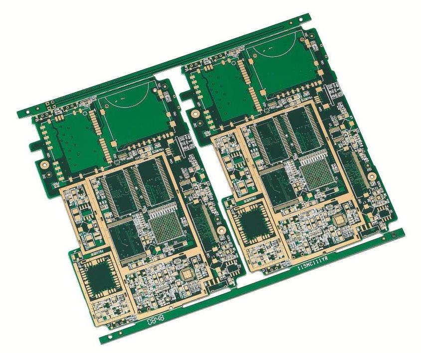
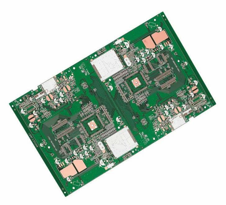
1.1 Production board
Any PCB board that meets the design drawings, relevant specifications, and procurement requirements and is produced in one production batch
1.2 As received
The product submitted for acceptance has not been subjected to any conditioning treatment, and it is in the state of mechanical testing under normal atmospheric conditions.
1.3 test board
A printed board is produced by the same process and used to determine the acceptability of a batch of printed boards. It represents the quality of the batch of printed boards
1.4 Test pattern
A conductive pattern is used to complete a test. The pattern can be a part of the conductive pattern on the production board or a specially designed special test pattern. This test pattern can be placed on the attached test board. The liquid can be placed on a separate test board
1.5 Composite test pattern
A combination of two or more different test patterns, usually placed on a test board
1.6 Quality conformance test circuit
A complete set of test patterns is included in the build to determine the acceptability of the printed board quality on the build
1.7test coupon attached test board
A drawing of a portion of a quality conformance test circuit used for a specified acceptance test or set of related tests
1.8 Storage life

2. Appearance and size
2.1 Visual examination
Examination of physical features with the naked eye or at specified magnifications
2.2 Blister
The phenomenon of local separation is caused by local expansion between the layers of the substrate or between the substrate and the conductive foil, between the substrate and the protective coating, which is a form of delamination
2.3 Blow hole
Holes due to exhaust
2.4 Bulge
Bumping on the surface of a printed board or foil clad due to internal delamination or separation of fibers from resin
2.5 Circumferential separation
A crack or void. It exists in the plating around a plated-through hole, in a solder joint around a lead, in a solder joint around a hollow rivet, or at the interface of a solder joint and a land
2.6 Cracking
A phenomenon of breakage in a metallic or non-metallic layer that may extend all the way to the bottom.
2.7 Crazing
A phenomenon exists in a substrate where the glass fibers separate from the resin at the interlacing of the fabric. It is manifested as connected white spots or crosses under the surface of the substrate, usually related to mechanical stress
2.8 Measling
The phenomenon that occurs inside the substrate, where the fabric is interwoven, the glass fiber and the resin are separated, which manifests as scattered white spots or cross patterns under the surface of the substrate, usually related to thermal stress.
2.9 Crazing of conformal coating
Microscopic cracks appear on the surface and inside of the conformal coating
2.10 Delamination
The interlayer of insulating substrates, the phenomenon of insulating substrates and conductive foils, or an interlayer separation within a multilayer board
2.11 Dent
Smooth depressions on the surface of the conductive foil that do not significantly reduce its thickness
2.12 Estraneous copper
Unwanted copper remaining on substrate after chemical treatment
2.13 Fibre exposure
Reinforcing fibers exposed to the substrate due to mechanical processing or abrasion or chemical attack
2.14 Weave exposure
A condition on the surface of a substrate in which unbroken woven glass fibers in the substrate are not completely covered by resin
2.15 Weave texture
A condition on the surface of the substrate, that is, the fibers of the woven glass cloth in the substrate are not broken and are completely covered by resin, but the weave pattern of the glass cloth is displayed on the surface
2.16 Wrinkle
Creases or wrinkles on the foil surface
2.17 Haloing
Destruction or delamination on or under the surface of a substrate due to machining. Usually manifested as whitish areas around holes or other machined areas
2.18 Hole breakout
The phenomenon that the connection plate does not completely surround the hole
2.19 Flare
In punching engineer, the tapered hole formed in the substrate on the exit face of the punch
2.20 Splay
Rotary drill to produce eccentric, out-of-round, or non-perpendicular holes
2.21 Void
Lack of substances in the local area
2.22 Hole void
A hole that exposes the substrate within the metallization of the plated-through hole
2.23 Inclusion
Foreign particles trapped in substrates, wire layers, plating coatings, or solder joints
2.24 Lifted land
The phenomenon that the land is lifted or separated from the substrate, regardless of whether the resin is lifted from the land
2.25 Nail heading
The phenomenon that the copper foil on the inner conductor is stretched along the hole wall due to drilling in the multilayer board
2.26 Nick
2.27 Node
Irregular lumps or nodules protruding from the surface of the coating
2.28 Pinhole
A hole that completely penetrates a layer of metal
2.30 Resin recession
The cavity between the plated-through hole wall and the drilled hole wall can be seen from the microsection of the plated-through hole of the printed board after being subjected to high temperature
2.31 Scratch
2.32 bump
Protrusions on the surface of the conductive foil
2.33 Conductor thickness
2.34 Minimum annular ring
2.35 Registration
Consistency of the location of graphics, holes, or other features on the printed board with the specified locations
2.36 Base material thickness
2.37 Metal-clad laminate thickness
2.38 Resin starved area
The part of the laminate that fails to fully infiltrate the reinforcing material due to insufficient resin. It shows poor gloss, the surface is not completely covered by the resin or the fibers are exposed
2.39 Resin-rich area
The part of the laminate surface where the resin thickens significantly where there is no reinforcement, that is, the area with resin but no reinforcement
2.40 Gelation particle
Cured, usually translucent particles in laminate
2.41 Treatment transfer
The phenomenon in which the copper foil treatment layer (oxide) is transferred to the substrate. After the surface copper foil is etched away, black, brown, or red traces remain on the surface of the substrate.
2.42 Printed board thickness
The total thickness of the substrate and conductive material (including plating) overlying the substrate
2.43 Total board thickness
The thickness of the printed board including the electroplating layer the electroplating layer and other coating layers that form a whole with the printed board
2.44 Rectangularity
The offset of the corners of the rectangular plate from 90 degrees
3. Electrical properties
3.1 Contact resistance
Withstand surface resistance at the contact interface measured under specified conditions
3.2 Surface resistance
The quotient of the DC voltage between two electrodes on the same surface of an insulator divided by the steady-state surface current developed between the two electrodes
3.3 Surface resistivity
The quotient of the DC electric field strength at the surface of the insulator divided by the current density
3.4 Volume resistance
The quotient was obtained by dividing the DC voltage applied between two electrodes on the opposite surfaces of the sample by the steady-state surface current formed between the two electrodes
3.5 Volume resistivity
The quotient of the DC electric field strength in the sample divided by the steady-state current density
3.6 Dielectric constant
The ratio of the capacitance obtained by filling the dielectric between the electrodes of the specified shape to the capacitance when the same electrodes are in a vacuum
3.7 Dielectric dissipation factor
When a sine wave voltage is applied to a dielectric, the complementary angle of the phase angle between the current phasor leading through the dielectric and the voltage phasor is called the loss angle. The tangent of the loss angle is called the loss factor
3.8 Q factor
A quantity for evaluating the electrical properties of a dielectric. Its value is equal to the reciprocal of the dielectric loss factor
3.9 Dielectric strength
The voltage that the insulating material can withstand before breakdown per unit thickness
3.10 Dielectric breakdown
The phenomenon that insulating materials completely lose their insulating properties under the action of an electric field
3.11 Comparative tracking index
Under the combined action of the electric field and the electrolyte, the surface of the insulating material can withstand 50 drops of the electrolyte without the formation of electrical traces.
3.12 Arc resistance
The ability of an insulating material to withstand the action of an electric arc along its surface under specified test conditions. Usually, the time required for the arc to cause carbonization on the surface of the material until the surface conducts electricity
3.13 Dielectric withstanding voltage
The voltage that an insulator can withstand without breaking the insulation and conducting current
3.14 Surface corrosion test
Test to determine the presence or absence of electrolytic corrosion of etched conductive patterns under polarized voltage and high humidity conditions
3.15 Electrolytic corrosion test at the edge
Test to determine whether a substrate will cause corrosion of metal parts in contact with it under conditions of polarization voltage and high humidity
4. Non-electrical properties
4.1 Bond strength
Force per unit area normal to the surface of a printed board or laminate required to separate adjacent layers of a printed board or laminate
4.2 Pull off strength
The force required to separate the land from the substrate when a load or tension is applied in the axial direction
4.3 Pullout strength
The force required to separate the metal layer of a plated-through hole from the substrate when a tensile force or load is applied in the axial direction
6.4.5 Peel strength
The force perpendicular to the board surface is required to peel off a unit width of wire or metal foil from a foil-clad board or printed board
6.4.6 Bow
A deformation of a laminate or printed board to a plane. It can be roughly represented by the curvature of a cylindrical or spherical surface. If it is a rectangular plate, its four corners are in the same plane when it is bowed
4.7 Twist
Deformation of the plane of a rectangular plate. One of its corners is not in the plane containing the other three corners
4.8 Camber
The degree to which the plane of a flex board or flat cable deviates from a straight line
4.9 Coefficient of thermal expansion (CTE)
Linear change in material size per unit temperature change
4.10 Thermal conductivity
Unit time and unit temperature gradient, the heat that flows vertically through the unit area and unit distance
4.11 Dimensional stability
A measure of dimensional change caused by factors such as temperature, humidity, chemical treatment, aging, or stress
4.12 Solderability
The ability of metal surfaces to be wetted by molten solder
4.13 Wetting
Molten solder coats the base hole metal to form a fairly uniform, smooth, and continuous film of solder
4.14 Dewetting
After the molten solder covers the surface of the base metal, the solder shrinks, leaving irregular solder bumps, but the base metal is not exposed
4.15 Nowetting
The phenomenon in which molten solder contacts the metal surface and only partially adheres to the surface, leaving the base metal exposed
4.16 Ionizable contaminants
Residuals during processing can form polar compounds that can dissolve in water as free ions, such as flux activators, fingerprints, etching solutions or electroplating solutions, etc. When these contaminants dissolve in water, the resistivity of water decreases.
4.17 Microsectioning
For the golden image inspection of the material, the method of preparing the sample in advance. It is usually made by cutting the section, then pouring glue, grinding, polishing, etching, dyeing, etc.
4.18 Plated through hole structure test
Visual inspection of metal wires and plated-through holes after dissolving the substrate of the printed board
4.19 Solder float test
Float the sample on the molten solder surface for a specified time at a specified temperature to test the ability of the sample to withstand thermal shock and high temperature
4.20 Machinability
The ability of foil-clad laminates to withstand drilling, sawing, punching, shearing, etc. machining without breaking, shattering, or other damage
4.21 Heat resistance
The ability of a foil-clad sheet sample to be placed in an oven at a specified temperature for a specified period of time without blistering
4.22 Hot strength retention
The strength of a laminate in the hot state as a percentage of its strength in the normal state
4.23 Flexural strength
The stress that a material can withstand when it reaches a specified deflection or ruptures under a bending load
4.24 Tensile strength
Under the specified test conditions, the tensile stress that can be endured when a tensile load is applied to the sample
4.25 Elongation
When the specimen breaks under tensile load, the ratio of the increment of the distance between the marking lines in the effective part of the sample to the initial marking line distance
4.26 Tensile modulus of elasticity
The ratio of the tensile stress experienced by the material to the corresponding strain produced by the material within the elastic limit
4.27 Shear strength
The stress per unit area of a material when it breaks under shear stress
4.28 Tear strength
The force required to split the plastic film into two parts. The sample with no slit is called the initial tear strength, and the sample with a slit is called the expanded tear strength
4.29 Cold flow
Deformation of a non-rigid material under continuous load over the operating range
4.30 Flammability
The ability of a material to burn with flame under specified test conditions. In a broad sense, it includes the flammability and continual combustion of the material
4.31 Flaming combustion
Luminescent combustion of the sample in the gas phase
4.32 Glowing combustion
The sample does not burn with flame, but the surface of the burning area can be electrocuted by visible light
4.33 Self-extinguishing
Under the specified test conditions, the material stops burning after the ignition source is removed
4.34 Oxygen index (OI)
Under the specified conditions, the oxygen concentration is required for the sample to maintain flame combustion in the oxygen-nitrogen mixed gas flow. Expressed as the volume percentage of oxygen
4.35 Glass transition temperature
The temperature at which an amorphous polymer changes from a glassy brittle state to a viscous-fluid or highly elastic state
4.36 Temperature index (TI)
The value in degrees Celsius corresponding to a given time (usually 20,000 hours) on the thermal life graph of the insulating material
4.37 Fungus resistance
Material resistance to mold
4.38 Chemical resistance
The resistance of the material to the action of acid, alkali, salt, solvent, and it's steam and other chemical substances. It is expressed as the degree of change in the weight, size, appearance, and other mechanical properties of the material.
4.39 Differential scanning calorimetry
A technique for measuring the power difference input to a substance and a reference as a function of temperature at a programmed temperature
4.40 Thermal mechanical analysis
A technique for measuring the temperature dependence of the deformation of a material under non-vibration loading at a programmed temperature
5. Prepreg materials and adhesive films
5.1 Volatile content
The content of volatile substances in the prepreg material or the glue-coated film material is expressed as the percentage of the mass of the volatile substances in the sample to the original mass of the sample
5.2 Resin content
The content of the resin in the laminate or prepreg expressed as a percentage of the mass of the resin in the sample to the original mass of the sample
5.3 Resin flow
Properties of prepreg or B-stage adhesive film to flow under pressure
5.4 Gel time
The time, in seconds, required for a prepreg or B-stage resin to pass from a solid to a liquid to a solid under the action of heat
5.5 Tack time
When the prepreg is heated at a predetermined temperature, the time required from the start of heating until the resin melts and reaches a viscosity sufficient for continuous drawing
5.6 Prepreg cured thickness
The average sheet thickness was calculated by pressing the prepreg into a laminate under the specified temperature and pressure test conditions on PCB board