This article will elaborate on some manufacturing process issues that need to be considered when designing through-hole PCB board and provide a reference for designers. Design for manufacturability is a novel design method. It guarantees the quality of the production process and helps to improve production efficiency.
1 Introduction
For electronic product designers, especially circuit board designers, the manufacturability design of products is a factor that must be considered. If the PCB board design does not meet the manufacturability design requirements, the production efficiency of the product will be greatly reduced, and in severe cases, the designed product may not be manufactured at all. Through-hole technology is still in use today, and DFM can play a big role in improving the efficiency and reliability of through-hole manufacturing. DFM methods can help through-hole manufacturers reduce defects and remain competitive. This article introduces some DFM methods related to through-hole insertion. These principles are general in nature, but not necessarily applicable in all situations. However, PCB board designers and engineers working with through-hole technology Said it was still helpful.

2. Typesetting and layout
Proper layout during the design phase can save many of the hassles of the manufacturing process.
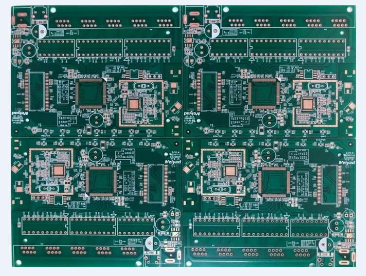
1) Using a large board can save materials, but it will be difficult to transport in production due to warpage and weight. It needs to be fixed with a special fixture, so try to avoid using a board surface larger than 23×30cm. It is to control the size of all boards within two or three, which helps to shorten the downtime caused by adjusting the guide rails, rearranging the position of the barcode reader, etc. when the product is changed, and the small variety of board sizes can also reduce the wave peak The number of solder temperature profiles.
2) It is a good design method to include different kinds of puzzles in one board, but only those boards that end up in one product and have the same production requirements can be designed this way.
3) Some borders should be provided around the board, especially when there are components on the edge of the board, most automatic assembly equipment requires at least a 5mm area on the edge of the board.
4) Try to make wiring on the top surface (component surface) of the board, the bottom surface (soldering surface) of the circuit board is easily damaged. Do not route wiring close to the edge of the board, because the production process is gripped by the edge of the board, and the wiring on the edge can be damaged by the jaws of the wave soldering equipment or the frame conveyor.
5) For devices with higher pin counts such as headers or flat cables, oval pads should be used instead of round to prevent solder bridging during wave soldering (Figure 1).
6) Make the spacing of the positioning holes and the distance between them and the components as large as possible, and standardize and optimize the size according to the insertion equipment; do not electroplate the positioning holes, because of the diameter of the electroplating holes is difficult to control.
7) Try to use the positioning hole as the mounting hole of the PCB board in the final product, which can reduce the drilling process during production.
8) A test circuit pattern can be arranged on the waste side of the board for process control, which can be used to monitor surface insulation resistance, cleanliness, solderability, etc. during manufacturing.
9) For larger boards, a passage should be left in the center to support the circuit board at the center position during wave soldering, to prevent the board from sagging and solder sputtering, and help the board surface to be soldered consistently.
10) The testability of the bed of needles should be considered in the layout design. Flat pads (without leads) can be used for a better connection with the pins during online testing so that all circuit nodes can be tested.
3. Positioning and placement of components
1) Arrange components in rows and columns according to a grid pattern position, all axial components should be parallel to each other, so that the axial insertion machine does not need to rotate the PCB board when inserting because of unnecessary rotation and movement will greatly Decrease the speed of the inserter.
2) Similar elements should be laid out in the same way on the board. For example, make the negative poles of all radial capacitors face the right side of the board, make all the notch marks of the dual in-line package face the same direction, etc., which can speed up the insertion speed and make it easier to find errors. As shown in Figure 3, since the A board adopts this method, the reverse capacitor can be easily found, while the B board search takes more time. Actually, a company can standardize the orientation of all circuit board components it manufactures, some board layouts may not necessarily allow this, but it should be an effort.
3) Align the orientation of dual in-line package components, connectors, and other high-pin-count components with the direction of wave soldering, which can reduce solder bridges between component pins.
4) Make full use of silk screen printing to mark the board, such as drawing a frame for sticking barcodes, printing an arrow to indicate the direction of wave soldering of the board, and using dotted lines to trace the outline of the components on the bottom surface (so that the board only needs to be screen printed), etc. Wait.
5) Drawing the component reference and polarity indication and still visible after component insertion is helpful during inspection and troubleshooting, and is also a good maintenance job.
6) The distance between the components and the edge of the board should be at least 1.5mm (3mm), which will make the circuit board easier to transmit and wave solder, and the damage to the peripheral components will be less.
7) When the distance between the components above the board surface needs to exceed 2mm (such as light-emitting diodes, high-power resistors, etc.), spacers should be added below them. Without spacers, these elements would be "squashed" during transport and would be susceptible to shock and shock during use.
8) Avoid placing components on both sides of the PCB, as this will greatly increase assembly labor and time. If components must be placed on the bottom surface, they should be physically close together to allow masking and stripping of the solder mask tape.
9) Try to distribute components evenly on the PCB to reduce warpage and help distribute heat evenly during wave soldering.
4. Machine insertion
1) Pads for all components on the board should be standard and industry standard separation distances should be used.
2) The selected components should be suitable for machine insertion. Keep in mind the conditions and specifications of the equipment in your factory, and consider the packaging form of the components in advance to better match the machine. For odd-shaped components, packaging can be a bigger problem.
3) If possible, use the axial type of the radial element as much as possible, because the insertion cost of the axial element is relatively low, and if the space is very precious, the radial element can also be preferred.
4) If there are only a small number of axial elements on the board, they should all be converted to radial types, and vice versa, so that an insertion process can be completely eliminated.
5) When arranging the board surface, the bending direction of the pins and the range reached by the components of the automatic insertion machine should be considered from the perspective of electrical spacing, and at the same time, it should be ensured that the bending direction of the pins will not lead to tin bridges.
5. Wires and connectors
1) Do not connect wires or cables directly to the PCB, but use connectors. If the wire must be soldered directly to the board, the end of the wire should be terminated with a wire to the terminal of the board. The wires coming out of the circuit board should be concentrated in a certain area of the board so that they can be nested together to avoid affecting other components.
2) Use wires of different colors to prevent errors in the assembly process. Each company can adopt its own set of color schemes, such as the high bits of all product data lines are represented by blue and the low bits are represented by yellow, etc.
3) Connectors should have larger pads to provide better mechanical connection, and the leads of high pin count connectors should be chamfered for easier insertion.
4) Avoid the use of dual in-line package sockets, which in addition to extending assembly time, this additional mechanical connection will reduce long-term reliability, and sockets are only used when DIP field replacement is required for maintenance reasons. The quality of DIPs has come a long way today and does not require frequent replacement.
5) Marks for identifying the direction should be engraved on the board to prevent errors when installing the connector. Connector solder joints are places where mechanical stress is concentrated, so it is recommended to use some clamping tools, such as keys and snaps.
6. Whole system
1) Components should be selected prior to designing a printed circuit board, which enables layout and helps implement the DFM principles described in this article.
2) Avoid using some parts that require machine pressure, such as wire pins, rivets, etc. In addition to slow installation, these parts may damage the circuit board, and they are also low maintenance.
3) Use the following methods to minimize the types of components used on the board: replace a single resistor with a row resistor; replace two three-pin connectors with a six-pin connector; if the values of the two components are similar, but the tolerances are different, Then use the one with the lower tolerance in both locations; use the same screws to secure the various heatsinks on the board.
4) Designed as a general purpose board that can be configured in the field. Such as installing a switch to change the board used in China to the export model, or using jumpers to change one model to another.
7. General requirements
1) When the conformal coating is applied to the circuit board, the part that does not need coating should be marked on the drawing during engineering design, and the influence of the coating on the capacitance between wires should be considered during design.
2) For through holes, in order to ensure the welding effect, the gap between the pin and the aperture should be between 0.25mm and 0.70mm. A larger pore size is beneficial for machine insertion, while smaller pore size is required for good capillary effect, so a balance needs to be struck between the two.
3) Components that have been pretreated according to industry standards should be selected. Component preparation is one of the efficient parts of the production process, and in addition to adding additional steps (with a corresponding risk of electrostatic damage and longer lead times), it also increases the chance of error.
4) Specifications should be set for most of the purchased hand-inserted components so that the length of the lead on the soldering surface of the circuit board does not exceed 1.5mm, which can reduce the workload of component preparation and pin trimming, and the board can be better ground through the wave soldering equipment.
5) Avoid using snaps to install smaller mounts and radiators, as this is very slow and requires tools, and should try to use sleeves, plastic quick-connect rivets, double-sided tapes, or use solder joints for mechanical connections on PCB board.