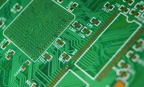
1. Basic concept of via
Through hole is an important part of a multilayer PCB board, and the cost of drilling usually accounts for 30% to 40% of the cost of PCB manufacturing. In short, each hole on a PCB can be called a through hole. From the perspective of function, vias can be divided into two categories: one is used as electrical connection between layers; Second, it is used for fixing or positioning devices. In terms of process, these vias are generally divided into three categories, namely blind hole, buried hole and through hole. The blind hole is located on the top and bottom surfaces of the printed circuit board, and has a certain depth. It is used to connect the surface line and the lower inner line. The depth of the hole usually does not exceed a certain ratio (aperture). Embedded hole refers to the connection hole located in the inner layer of the printed circuit board, which will not extend to the surface of the printed circuit board. The above two types of holes are located in the inner layer of the circuit board. Before lamination, the through hole forming process is used to complete the hole. During the hole forming process, several inner layers may be overlapped. The third is called through hole, which passes through the whole circuit board and can be used for internal interconnection or as the installation and positioning hole of components. Because the through-hole is easier to realize in technology and lower in cost, most printed circuit boards use it instead of the other two kinds of through-hole. The following vias, unless otherwise specified, are considered as through-hole. From the design point of view, a via is mainly composed of two parts: one is the middle drill hole, and the other is the pad area around the drill hole. The size of these two parts determines the size of the vias. Obviously, when designing high-speed and high-density PCB boards, designers always hope that the smaller the vias are, the better, so that more wiring space can be left on the board. In addition, the smaller the via, the smaller its parasitic capacitance, which is more suitable for high-speed circuits. However, the reduction of hole size also brings about an increase in cost, and the size of vias cannot be reduced without limitation. It is limited by drilling and electroplating technology: the smaller the hole, the longer the drilling time will take, and the easier it is to deviate from the center; And when the depth of the hole exceeds 6 times of the drilling diameter, it is impossible to ensure that the hole wall can be uniformly copper plated. For example, if the thickness (through-hole depth) of a normal 6-layer PCB is 50Mil, then under normal conditions, the diameter of the hole provided by the PCB manufacturer can only reach 8Mil. With the development of laser drilling technology, the size of drilling can also be smaller and smaller. Generally, vias with a diameter of less than or equal to 6Mils are called micropores. Microholes are often used in HDI (high-density interconnection structure) design. Microhole technology allows vias to be directly punched on pads, which greatly improves circuit performance and saves wiring space. The vias on the transmission line behave as breakpoints with discontinuous impedance, which will cause signal reflection. Generally, the equivalent impedance of the vias is about 12% lower than that of the transmission lines. For example, the impedance of a 50 ohm transmission line will decrease by 6 ohm when it passes through the vias (specifically related to the size of the vias and the thickness of the plates, not the reduction). However, the reflection caused by the discontinuous impedance of vias is actually very small, and its reflection coefficient is only (44-50)/(44+50)=0.06. The problems caused by vias are more concentrated on the effects of parasitic capacitance and inductance.

2. Parasitic capacitance and inductance of via
There is parasitic stray capacitance in the via itself. If it is known that the diameter of the solder mask area of the via on the floor is D2, the diameter of the via pad is D1, the thickness of the PCB is T, and the dielectric constant of the board substrate is ε, Then the parasitic capacitance of the via is approximately C=1.41 ε The parasitic capacitance of TD1/(D2-D1) via will mainly affect the circuit by prolonging the signal rise time and reducing the circuit speed. For example, for a PCB with a thickness of 50Mil, if the via pad diameter is 20Mil (drilling diameter is 10Mils) and the solder mask area diameter is 40Mil, we can approximately calculate the parasitic capacitance of the via through the above formula: C=1.41x4.4 x 0.050 x 0.020/(0.040-0.020)=0.31pF The rise time change caused by this part of capacitance is approximately T10-90=2.2C (Z0/2)=2.2x0.31x (50/2)=17.05ps. It can be seen from these values that although the effect of the rise delay caused by the parasitic capacitance of a single via is not very obvious, if the via is used for inter layer switching for many times in the routing, multiple vias will be used, which should be carefully considered in the design. In practical design, parasitic capacitance can be reduced by increasing the distance between via and copper clad area or reducing the diameter of pad. Parasitic capacitance and inductance exist in vias. In the design of high-speed digital circuits, the parasitic inductance of vias often brings more harm than the parasitic capacitance. Its parasitic series inductance will weaken the contribution of bypass capacitor and the filtering effectiveness of the whole power supply system. We can use the following empirical formula to simply calculate the approximate parasitic inductance of a via: L=5.08h [ln (4h/d)+1] where L is the inductance of the via, h is the length of the via, and d is the diameter of the central borehole. It can be seen from the formula that the diameter of the via has little influence on the inductance, while the length of the via has little influence on the inductance. Using the above example, it can be calculated that the inductance of the via is: L=5.08x0.050 [ln (4x0.050/0.010)+1]=1.015nH If the rise time of the signal is 1ns, the equivalent impedance is XL=π L/T10-90=3.19 Ω. Such impedance cannot be ignored when there is high-frequency current passing through. In particular, the bypass capacitor needs to pass through two vias when connecting the power layer and the stratum, so the parasitic inductance of the vias will be multiplied.
3. How to use vias
Through the above analysis of the parasitic characteristics of vias, we can see that in high-speed PCB design, seemingly simple vias often bring great negative effects to circuit design. In order to reduce the adverse effects caused by the parasitic effect of vias, the following measures can be taken in the design:
1) Considering the cost and signal quality, the reasonable size of vias is selected. If necessary, you can consider using vias of different sizes. For example, for power supply or ground wire vias, you can consider using larger sizes to reduce impedance, while for signal wiring, you can use smaller vias. Of course, with the reduction of via size, the corresponding cost will increase.
2) From the two formulas discussed above, it can be concluded that the use of thinner PCB is beneficial to reduce the two parasitic parameters of vias.
3) The signal wiring on the PCB shall not change layers as much as possible, that is to say, unnecessary vias shall not be used as much as possible.
4) The pins of power supply and ground shall be punched nearby, and the lead between the via and pin shall be as short as possible. Multiple vias can be drilled in parallel to reduce the equivalent inductance.
5) Place some grounded vias near the vias for signal layer change, so as to provide near circuit for signals. You can even place some redundant grounding vias on the PCB.
6) For high-speed PCB boards with high density, micro vias can be considered.