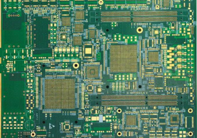
Why are most multilayer PCB even? There are few odd layers. For these reasons, PCB board is divided into single-sided, double-sided and multi-layer. There is no limit to the number of layers of multilayer PCB. At present, there are 100 multilayer PCB, and the common multilayer PCB is four layer and six layer board.
Comparatively speaking, even number PCB board has more advantages than odd number PCB board. Due to the lack of a layer of medium and foil, the raw material cost of odd PCB is slightly lower than that of even PCB. However, the processing cost of odd PCB is significantly higher than that of even PCB. The processing cost of the inner layer is the same, but the foil/core structure significantly increases the processing cost of the outer layer.
1) Non standard laminated core bonding process should be added to the core structure process of odd PCB. Compared with the core structure, the production efficiency of the factory adding foil outside the core structure will be reduced. Before laminated bonding, the outer core requires additional process treatment, which increases the risk of scratches and etching errors.
2) The balanced structure avoids bending. The best reason to design a PCB without odd layers is that the odd layers of the PCB are easy to bend. After the multilayer circuit bonding process is completed, when the PCB is cooled, different laminating tensions will cause the PCB to bend when the core structure and foil structure are cooled. With the increase of PCB thickness, the bending risk of composite PCB with two different structures is greater. The key to eliminate PCB bending is to use balanced lamination. Although the bent PCB meets the specification requirements to a certain extent, the subsequent processing efficiency will be reduced, resulting in increased costs. Due to the special equipment and process required in the assembly process, the placement accuracy of parts will be reduced, thus affecting the quality. In other words, it is easier to understand: in the PCB process, the four layer board is easier to control than the three layer board. In terms of symmetry, the warpage of the four ply board can be controlled below 0.7% (ipc-a-600 specifications), but when the size of the three ply board is large, the warpage will exceed this standard, which will affect the reliability of the SMT patch and the entire product. Therefore, the chief designer will not design odd number of laminates. Even if the odd number layer realizes this function, it will also be designed as a pseudo even number layer, that is, 5 layers are designed as 6 layers, and 7 layers are designed as 8 layers. For the above reasons, most PCB multilayer PCB is designed with even layers and few odd layers.

If we compare a single panel of a PCB with the multilayer PCB, we can see the difference on the surface without discussing its internal quality. These differences are very important for the durability and functionality of PCB board throughout their service life. The main advantage of the multilayer PCB board is that the circuit board has oxidation resistance. Various structures, high density and surface coating technologies ensure the quality and safety of the printed circuit boards, which can be used safely. The following are the important features of high reliability multilayer boards, that is, the advantages and disadvantages of multilayer PCB:
1) The copper thickness of hole wall of multilayer PCB is 25 μm normally;
Advantages: Enhanced reliability, including improved z-axis extension resistance.
Disadvantages: but there are also certain risks: under the actual use, the electrical connectivity (inner layer separation, hole wall fracture) during blowing out or degassing, assembly, or the possibility of failure under load conditions. IPC Class2 (the standard of most factories) requires that the copper plating of multilayer PCB should be less than 20%.
2) No welding repair or open circuit repair
Advantages: The perfect circuit ensures reliability and safety without maintenance and risk.
Disadvantages: If the maintenance is improper, the multilayer PCB is open. Even if properly fixed, there may be a risk of failure under load conditions (vibration, etc.), which may lead to failure in actual use.
3) Cleanliness requirements exceeding IPC specifications
Advantages: The reliability can be improved by improving the cleanliness of multilayer PCB.
Risk: The residue on the terminal block and the accumulation of solder will bring risks to the anti welding layer, and the ionic residue will lead to the risk of corrosion and contamination of the welding surface, which may lead to reliability problems (poor welding contact/electrical failure) and ultimately increase the probability of actual failure.
4) Strictly control the service life of each surface treatment
Advantages: Welding, reliability and reduced risk of moisture intrusion.
Risk: It is the surface treatment of the old multilayer PCB that may lead to metallographic changes and may have soldering problems, while water intrusion may lead to problems in the assembly process and/or the actual use of delamination, separation (open circuit) of the inner wall and wall, etc.
No matter in the PCB manufacturing and assembly process or in actual use, multilayer PCB must have reliable performance, of course, this is related to the equipment, process and technology level of PCB board printing plants.