1. First trial production and test welding
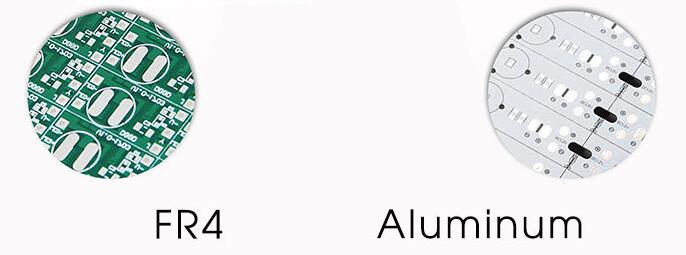
(1) fr4 pcb structure and soldering back
First of all, the FR-4 plates hardened with high Tg and Dicy are made into two kinds of high multilayer plates of 22 layers and 24 layers. Using two kinds of reflow furnaces, the blank plates were simulated for 6-9 times under two kinds of L shaped reflow curves.

(2) Microsection analysis
After several times of back-welding and multiple plate bursts, the failure analysis was carried out for the plate burst zone. The following is the discovery of its equivalent section.
(3) Discussion
After the first reflow, we can see several representative logics: the reflow curve is easy to explode if the temperature rises too fast, and it is unknown whether the temperature drops too fast is related to the explosion. In addition, the author feels that the reflow curve used by the fr4 pcb company mentioned above is actually not appropriate. This kind of straight up and down curve without saddle heat absorption is only applicable to the reflow of low-order plates and simple parts. For complex multilayer, the curve of saddle or long saddle heat absorption section shall be adopted, so that the plate body is in the condition of internal and external uniform temperature, and then the welding can be completed by rapid uprush peak temperature action.
2. Second trial production and test welding
The plates in the second test have been mixed with different plates of Dicy and PN hardeners, and the results of this test show that the heat resistance of PN type is indeed better than Dicy. At the same time, it can also be seen that there are still some factors that affect the lead-free welding to cause the bursting of the plate: the pressing process, the baking after pressing, the water absorption of the inner layer plate, the water absorption of the finished plate, and the degree of resin polymerization. In the production process of fr4 pcb, two kinds of plates, Dicy hardening and PN hardening, were used for plate A. Although two different pressing processes were also selected, it was found that they had little effect on the results. On the contrary, the baking of the empty plate before welding has a direct impact on the bursting of the plate. The baking condition is 125 ℃ for a total of 24 hours. Now, the survival rate of its plates after lead-free back-welding is sorted out later.
(1) Discussion
When FR-4 is hardened by Dicy, its bursting phenomenon is almost simultaneous cracking at all parts of the whole plate, while when PN is hardened, local cracking occurs only in the porous area of the abdominal bottom. Dicy hardener will burst the plate after two times of back-welding, regardless of whether it is baked or not before back-welding. However, those hardened by PN and baked before welding can survive 50% after four times of reflow. It shows that Dicy is not easy to pass the test of thermal stress due to its large polarity and easy to absorb water. However, the polarity of PN is very small, the water absorption is very low, and the addition amount is more than 20% bywt. In fact, it has greatly changed the linear nature of epoxy resin, and has the three-dimensional structural strength of phenolic resin, so it is not easy to crack in strong heat.
3. Third trial production and test welding
(1) Preparation for test
In the third degree test, all the plates have been changed to hardened type, and the process of PCB board has been improved in particular. That is to say, in order to improve the yield of lead-free back-welding, all the finished inner plates are deliberately baked at 110 ℃ for 3 hours, and the outer plates are baked at 150 ℃ for 4 hours after removing the glue slag. As for the surface treatment, the eight plates of the 22 layers are electroplated nickel gold instead of ENIG. This time, a total of 6 batches of 15 boards were made in each batch, and 6 boards were deliberately baked at 125 ℃ for another 24 hours before reflow. The other six boards were deliberately not baked before reflow for comparison. In addition, two plates were taken from each of the two batches to carry out the following tests respectively: tin drift thermal stress test, Tg measurement, T260/T288 test, and simulated reflow of recovery welding curve 2. In this test, it was found that two types of PN-hardened plates were baked and not baked before welding. After 12 times of simulated back-welding, no plate burst occurred.
(2) Discussion of results
The test results of the six batches of boards mentioned above are summarized and discussed as follows: The six batches of PN-hardened boards can pass 12 times of simulated reflow regardless of whether they are baked twice in the PCB process. Three methods were used to test the △T of Tg1 and Tg2 before reflow. Although it was found that each △ T still had a difference of 1-8 ℃, its △ T did become much smaller after 12 reflow. That is to say, the hardening degree of the original resin is very good, which is directly related to the pressing process and baking after pressing. Since Tg2 is still higher than Tg1, it means that the resin in the plate has not been cracked yet. The T288 test was carried out after 12 times of back-welding, and it was found that the data obtained was not lower than the reading value before welding, which could also be interpreted as evidence that the resin had not been cracked. After three and six times of tin bleaching, all of them passed the test, and there was no blistering and bursting. Although there was also a hole ring floating due to CTE mismatch and resin shrinkage with volume shrinkage (not more than 20% of the hole length) on the slice, these were inevitable phenomena due to strong heat. As long as there was no micro-crack in the slice of the fr4 pcb plate, they could generally be regarded as acceptable small defects.