1. Aging of solder joint
After the completion of fr4 pcb welding, the crystal structure of the main alloy of the solder joint will not be stable and will gradually increase with time to reduce the internal stress caused by many boundaries (usually the boundaries are the concentration of impurities, high energy, and poor stability). Even at room temperature, the recrystallization temperature required for common eutectic alloys has been exceeded. As the grain size increases and the boundary decreases, the impurity concentration in the boundary increases relatively. Once the Fatigue life of the solder joint has consumed 25%, Microvoid will appear in the border. However, when the fatigue life is consumed by 40%, it will further deteriorate and produce microcrack, which will make the solder joint even weaker.

2. CTE mismatch
Once the CTE-mismatch difference of the overall thermal expansion coefficient of the three members (pin, solder, pad surface) is large, the deterioration of the strength of the solder joint will also accelerate. For example, the CTE of the ceramic BGA itself is 2ppm/℃, but the CTE of the FR-4 circuit board is 14ppm/℃. The welding strength between the two is not easy to be very good. As for the local CTE mismatch, it often occurs, such as 17 ppm/℃ for copper, 18 ppm/℃ for ceramics, and 20 ppm/℃ for Alloy42. However, the effect of the local CTE mismatch is slightly less than that of the above overall mismatch. Sometimes even the very homogeneous Sn63/Pb37 has tin and lead rich areas in its tissue (there will also be 6 ppm/℃ internal CTE-mismatch between them).
3. Example of failure mode
1) Cold welding
Refers to the solder paste on the fr4 pcb pad at the foot of the ball during Reflow, which is not completely fused with the ball due to insufficient heat. At this time, the spherical surface will present a rough granular appearance, and necking will also occur. Generally, the inner ball at the belly bottom is more prone to cold welding.
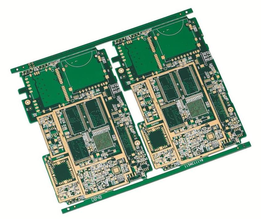
2) The solder pad itself is free of tin
It refers to that the surface of the ball pad in the BGA area of the PCB board is contaminated by foreign matters, so that the solder paste cannot react with the base pad. When the tin cannot be eaten, the solder paste will be melted and absorbed by the ball foot, resulting in an open circuit. However, this phenomenon may also be caused by the bending and warping of the carrier plate. When ENIG is used for PCB pad surface, the nickel-charged layer will also present the same adverse situation once black pad disease occurs.
3) Drop ball
It refers to that the BGA element was not firmly planted before, was reheated during downstream assembly and welding, and was pulled by external force and separated from its neck, which was caused by thermal mechanical stress. However, the foot pad of fr4 pcb is often well welded and less missing.
4) Concede a goal
The ball foot was not firmly planted in the process of ball planting on the carrier plate, or was later hit by an external force and lost the ball. This disadvantage can be easily found in X-Ray or system or circuit test (ICT), but if it is only used for heat
dissipation or common grounding, it does not matter the inner ball, it is another matter.
5) Carrier plate 'warping
In fact, in the future lead-free welding heat will increase greatly, not only the large fr4 pcb will be warped, but also the organic carrier plate itself will not be able to escape the warping deformation, and it will also force the abdominal bottom ball foot to fluctuate with height. Although the plate of the carrier plate is Tg180 BT resin, it is quite different from the CTE of the chip loaded in the inner seal; Therefore, when the lead-free heat is too much, the carrier plate will bend upward, causing the four corners of the ball feet to be stretched or suspended. Even if the weld is firmly welded, the welding contact area will become smaller and the strength will be insufficient due to the stress and elongation, which makes the designer dare not place 1/0 of the ball foot at the four corners. This kind of abnormal phenomenon is most likely to occur in large BGA.
6) Damage caused by external mechanical force
The circuit board often suffers accidental damage during assembly or test, and when BGA becomes large, the ball foot will also be injured during its test, which will affect the strength of subsequent solder joints. Even after completing the assembly of PCBA, it will still be accidentally impacted by external forces, and sometimes even the copper pad on the surface of PCB will be pulled up and floated away. For the sake of safety, we can use the bottom glue or the corner glue at the four corners as the means of security, or even increase the area of the corner pad or turn it into an oval long pad. However, because the designer only uses ready-made commercial software, this method is not easy to implement.
7) Insufficient welding heat
When the heat absorbed by the ball in the belly bottom is insufficient, the ball itself cannot melt into liquid, so that it cannot heal with the solder paste, and its fr4 pcb shape will be difficult to show the normal state of normal flattening and shortening.