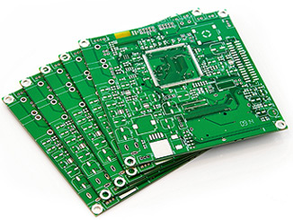
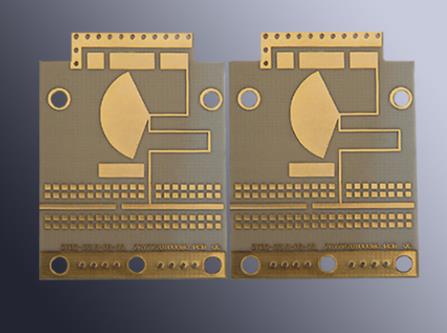
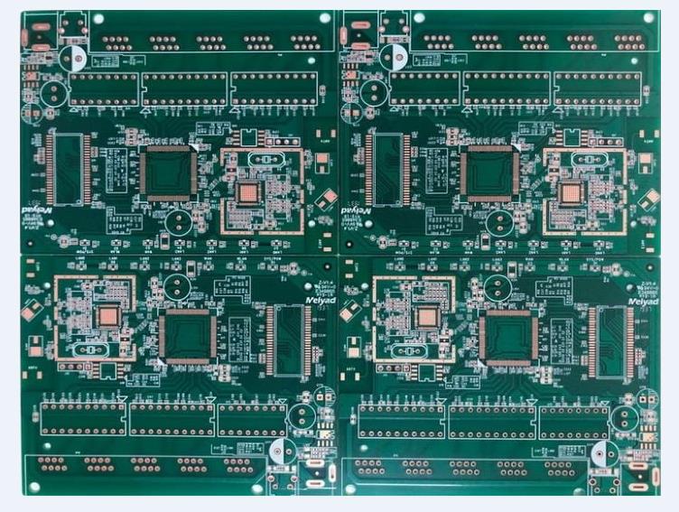
The through-hole solder paste is to print the solder paste directly on the Plating Through Hole of fr4 pcb, and then insert the traditional plug-in/DIP insert parts directly into the electroplated through-hole that has been printed with solder paste. At this time, most of the solder paste on the electroplated through-hole will stick to the solder pins of the plug-in parts. These solder pastes will melt again after the high temperature of the reflow furnace, and then weld the parts on the circuit board. There are other names for this method, such as pin-in-pate, invasive reflow consoling, ROT, reflow of through-hole, etc. The advantage of this method is that it can eliminate the process of hand soldering or wave soldering and thus save labor hours. At the same time, it can also improve the quality of welding and reduce the opportunity of solder short.

However, this method has the following congenital limitations:
The heat resistance of traditional parts must meet the temperature requirements of reflow soldering. General plug-in parts usually use materials with lower temperature resistance than reflow parts. Because this process requires that traditional parts and ordinary SMT parts be reflow welded together, it must meet the temperature resistance requirements of reflow. Lead-free parts can now withstand 260 ° C+10sec. The parts should have a tape-on-reel and enough plane to be placed on the fr4 pcb through the SMT pick and place machine. If not, it is necessary to consider sending an additional operator to manually place the parts. At this time, it is necessary to measure the required working hours and unstable quality, because the manual plug-in may touch other parts that have been placed and positioned due to careless operation. The solder pad between the part body and PCB should have a standoff design. Generally, the PIH process will print the solder paste larger than the outer frame of the solder pad. This is to increase the amount of solder paste to meet the 75% through-hole filling requirement. If there is no standoff between the part and the solder pad, the molten solder paste will travel along the gap between the part and the PCB during Reflow, and the early rainy solder slag and solder beads will affect the electrical quality in the future. It is better to make parts on the second side of traditional parts (if there are two SMTs). If the part has been punched on the first side, and the SMD continues to be punched on the second side, the solder paste may flow back into the traditional part, causing the possibility of internal short circuit of the part, especially the connector part. In addition, the amount of solder is the biggest challenge of this method. The acceptable standard solder amount of IPC-610 for through-hole welding points must be greater than 75% of the thickness of the carrier plate.
How can we increase the amount of solder? The following methods are for your reference:
Reserve enough space near the through hole of the circuit board for over print. Discuss with the wiring engineer that more space should be left for printing solder paste near the through-hole that needs paste-in-hole, that is to say, other pads or other unnecessary welding through-holes should not be placed nearby as far as possible to avoid short circuit when over printing. Note: The plane space of solder paste printing cannot be extended to the outside indefinitely. The cohesive force of solder paste must be considered, otherwise the solder paste will not be able to fully retract the solder pad and form solder beads. In addition, the direction of solder paste printing should match the direction of solder pad extension. Reduce the diameter of the through hole on the circuit board. Just like the above calculation of the amount of solder paste required, the larger the diameter of the through-hole, the more the amount of solder paste required, but at the same time, we should consider that if the diameter of the through-hole is too small, the parts will be inserted into the through-hole in Vietnam. Use step-up or step-down or stencil. This kind of steel plate can force local increase in the thickness of solder paste, which can also increase the amount of solder paste, so as to achieve the purpose of filling the through-hole with solder, but this kind of steel plate is about 10% more expensive than ordinary steel plate on average. Adjust the appropriate solder paste, the speed and pressure of the printer, the type and angle of the scraper, etc. These parameters of the solder paste printing machine will more or less affect the solder paste printing quantity. In addition, the solder paste quantity of the solder paste with a lower viscosity will be a little more. Add some solder paste. It can be considered to add some solder paste to the Paste-in-Hole solder pad to increase the amount of solder paste. Since there is almost no automatic dispenser in the SMT production line today, it can also be considered to manually dispense glue.
Test of the actual insertion function of the whole circuit board:
Generally, a complete machine product is composed of more than one circuit board. The so-called real insertion is to actually assemble all the circuit boards and parts needed to assemble a complete machine, but it does not need to be installed in the machine case. Because the function of the circuit board needs to be tested, it is necessary to make the printed circuit board easy to disassemble and assemble. As for the extent of actual plugging, it depends on which functions are tested. The ideal situation is that all functions can be tested. If not, most functions can also be tested. The key point should be to catch major problems, such as whether the power can be plugged in, whether the key functions are normal, and whether the screen displays normally. Otherwise, the test will be meaningless. Simply install the whole machine and test it again.
In addition, before starting the test, a set of circuit boards with normal functions should be prepared as standard templates. Suppose that a set of boards has three boards, A, B and C. When testing A boards, take out the B and C standard templates as fixtures, and only replace A boards for testing, so as to complete the test of three boards in turn. The biggest problem of this test method is that it is easy to damage the standard template. Because some connectors or flat cables between circuit boards cannot withstand too many times of plugging and unplugging, extended wiring is generally used. The advantage is that the extended wiring can be easily assembled, and all boards are not crowded together. In addition, the extended wiring is relatively cheap and easy to replace. If it is damaged, replace it, It is more cost-effective than using a bad circuit board. However, the functions of some components have special requirements for signals, so they cannot use extended wiring, such as barcode scanners, touch screens, etc. The need to spend a lot of time is also the disadvantage of this test method, so this method is usually only used in the case of small production quantities or the fr4 pcb design has not been finalized in the EVT (Engineer Verification Test) stage.