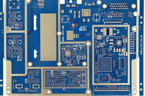
PCBA processing precautions and process
The anti-static precautions during PCBA processing are as follows:
1. All personnel who touch components and products wear anti-static clothes, anti-static bracelets, and anti-static shoes.
2. The anti-static system must have a reliable grounding device. The anti-static ground wire must not be connected to the power neutral wire or shared with the lightning protection ground wire.
3. All components are treated as electrostatic sensitive devices.
4. During the operation, use an anti-static work surface, and use anti-static containers for components and semi-finished products.
5. The welding equipment is firmly grounded, and the electric soldering iron is of anti-static type, which must be tested before use.
6. Warehouse management personnel should wear anti-static gloves when sending materials and IQC inspections, use meters to be grounded firmly, and have anti-static rubber pads on the work surface.
7. Regularly check the above-mentioned anti-static tools, settings and materials, and acknowledge that they are in the required conditions.

PCBA processing flow:
1. The customer provides engineering materials, including the review of BOM and Gerber documents, and then sorts out the set of bills to the purchasing department for component purchase;
2. Incoming inspection of components, inspection of qualified warehouses for storage, and warehouse preparations;
3. According to product characteristics and customer requirements, select PCB board/BGA/IC for baking to remove moisture;
4. Take out the solder paste, freeze and stir;
5. SMT patch;
6. Printing solder paste;
7. After the patch is completed, the board needs to be reflow soldered;
8. AOI inspection, first article inspection;
9. DIP plug-in, if the material requirements are shaped, it can be completed at this step;
10. The PCBA board with the inserted parts has been wave soldered;
11. AOI inspection, post welding processing;
12. Clean the PCBA board;
13. Conduct tests, mainly ICT and FCT tests. ICT is a circuit test, and FCT is a function test. To do a function test, customers need to provide a test plan;
14. Apply three-proof paint according to customer requirements, the main intention is to prevent moisture, moisture, and shock;
15. Product assembly (determine whether the demand is not required according to the customer's demand);
16. Pick the right packaging and pack it for shipment.
iPCB is happy to be your business partner. Our business goal is to become the most professional prototyping PCB manufacturer in the world. With more than ten years of experience in this field, we are committed to meeting the needs of customers from different industries in terms of quality, delivery, cost-effectiveness and any other demanding requirements. As one of the most experienced PCB manufacturers and SMT assemblers in China, we are proud to be your best business partner and good friend in all aspects of your PCB needs. We strive to make your research and development work easy and worry-free.
quality assurance
iPCB has passed ISO9001:2008, ISO14001, UL, CQC and other quality management system certifications, produces standardized and qualified PCB products, masters complex process technology, and uses professional equipment such as AOI and Flying Probe to control production and X-ray inspection machines. Finally, we will use double FQC inspection of appearance to ensure shipment under IPC II standard or IPC III standard.