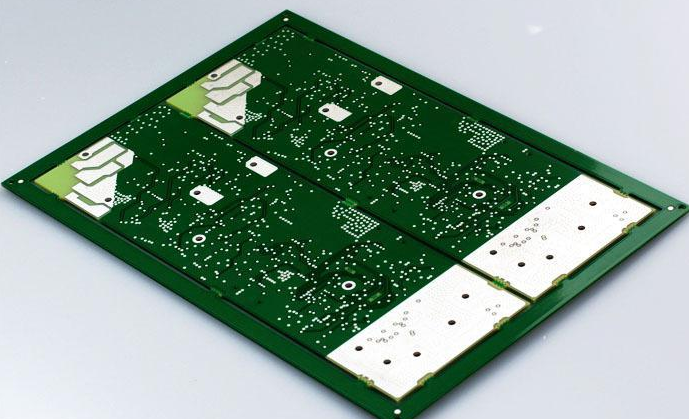
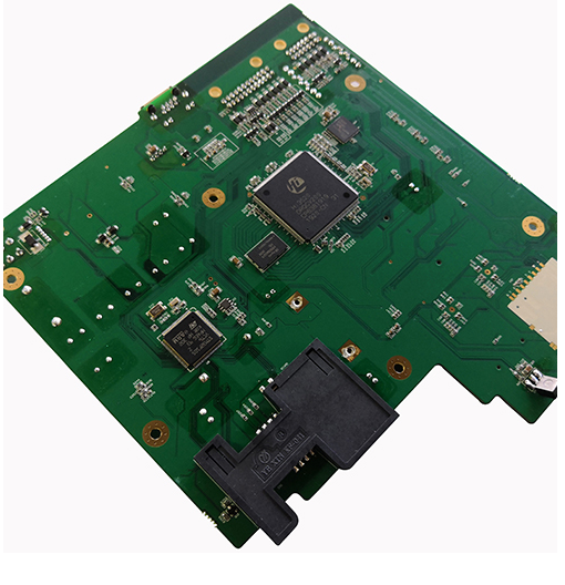
PCBA cleaning effect evaluation
1. PCBA pollution
Contaminants are defined as any surface deposits, impurities, slag inclusions and adsorbed substances that reduce the chemical, physical or electrical properties of PCBA to unqualified levels. There are mainly the following aspects:
1. The components that make up the PCBA, the pollution or oxidation of the PCB itself, etc. will cause the PCBA board surface pollution;
2. The residue produced by the flux during the manufacturing process is also the main pollutant;
3. Handprints, chain claws and jig marks produced during welding, and other types of pollutants, such as plugging glue, high temperature tape, handwriting and flying dust, etc.;
4. Dust, water and solvent vapors, smoke, tiny organic matter in the workplace, and the pollution caused by static electricity to attach to the PCBA.
2. The harm of pollution
Contamination may directly or indirectly cause PCBA potential risks, such as:
1. The organic acid in the residue may cause corrosion to PCBA;
2. During the electrification process, the electric ions in the residue cause electromigration due to the potential difference between the solder joints, which makes the product short-circuit and fail;
3. Residues affect the coating effect;
4. With time and environmental temperature changes, coating cracks and peeling will appear, which will cause reliability problems.

3. Typical problems of PCBA failure caused by pollution
1. Corrosion
PCBA assembly uses iron substrate bottom lead foot components. Due to the lack of solder bottom coverage, the iron substrate quickly produces Fe3+ under the corrosion of halogen ions and moisture, making the board surface red. In addition, in a humid environment, acidic ionic pollutants can directly corrode copper leads, solder joints and components, causing circuit failure.
2. Electromigration
If there is ionic contamination on the PCBA surface, electromigration is very easy to occur, and the ionized metal moves between the opposite electrodes and reduces to the original metal at the reverse end, resulting in a dendritic phenomenon called dendritic distribution, (dendritic, Dendrites, tin whiskers), the growth of dendrites may cause local short circuits in the circuit.
3. Poor electrical contact
In the PCBA assembly process, some resins such as rosin residues often contaminate the gold fingers or other connectors. When the PCBA is working hot or in a hot climate, the residues will become sticky, easy to absorb dust or impurities, and cause contact resistance to increase. Large or even open circuit failure. The corrosion of the nickel layer on the PCB surface pad in the BGA solder joint and the presence of the phosphorus-rich layer on the surface of the nickel layer reduce the mechanical bonding strength of the solder joint and the pad. Cracks occur when subjected to normal stress, resulting in point contact failure.
Fourth, the necessity of cleaning
1. Appearance and electrical performance requirements
The most intuitive effect of PCBA contamination is the appearance of PCBA. If it is placed or used in a high temperature and high humidity environment, the residue may absorb moisture and whiten. Due to the extensive use of leadless chips, micro-BGAs, chip-scale packaging (CSP) and 01005 in components, the distance between components and circuit boards is reduced, the size is miniaturized, and the assembly density is increasing. If the halide is hidden under the component where it cannot be cleaned, local cleaning may cause catastrophic consequences due to the release of halide.
2. Three anti-paint coating needs
Before the surface coating, the resin residue that has not been cleaned off will cause delamination or cracks in the protective layer; the active agent residue may cause electrochemical migration under the coating, leading to failure of the protection of the coating from cracking. Studies have shown that cleaning can increase the coating adhesion rate by 50%.
3. No-cleaning also needs to be cleaned
According to the current standard, the term "no-clean" means that the residues of the circuit board are safe from a chemical point of view, will not have any impact on the circuit board production line, and can be left on the circuit board. Corrosion, SIR, electromigration and other special detection methods are mainly used to determine the halogen halide content, and then to determine the safety of the no-clean assembly after the assembly is completed.
However, even if a no-clean flux with a low solid content is used, there will still be more or less residues. For products with high reliability requirements, no residues or contaminants are allowed on the circuit board. For military applications, even no-clean electronic assemblies are required to be cleaned.
Five, cleanliness requirements
Chinese PCB manufacturers face difficulties in choosing the level of cleanliness required to produce reliable hardware. The question of "how clean is enough clean" brings more challenges to narrower and narrower wires and lines. The cleanliness that is acceptable in one area of the industry (such as a toy after SMT processing) may be unacceptable in another area (such as flip chip packaging).
The following factors need to be considered:
1. End-use environment (aerospace, medical, military, automotive, information technology, etc.)
2. The design service cycle of the product (90 days, 3 years, 20 years, 50 years, shelf life +1 day)
3. The technology involved (high frequency, high impedance, power supply)
4. Products whose failure phenomenon corresponds to the terminal products 1, 2, and 3 defined by the standard (for example: mobile phones, heart rate regulators).
6. Qualitative and quantitative inspection of PCBA cleaning effect is evaluated by cleanliness index.
1. Cleanliness grade standards
According to the relevant regulations of the People’s Republic of China’s electronic industry military standard SJ20896-2003, according to the reliability and performance requirements of electronic products, the cleanliness of electronic products is divided into three levels, as listed in the table.
In actual work, it is practically impossible to eradicate pollution. A compromise is to determine the acceptable and unacceptable degree of pollution on the circuit board. According to IPC-J-STD-001 standard flux residue three-level standard regulations <40ugcm2, ionic pollutant content three-level standard regulations ≤1.5 (Nacl) ugcm2, extraction resistivity> 2*106Ω .cm
Please note that with the miniaturization of PCBA, this content is almost certainly too high. Commonly used ionic pollutants now require approximately ≤0.2 (Nacl) ugcm2.
2. Detection method of PCBA cleanliness
Visual inspection method: Use a magnifying glass or optical microscope to observe the PCBA, and evaluate the cleaning quality by observing whether there are solid flux residues, tin dross tin beads, unfixed metal particles and other contaminants. IPC-A-610 "Acceptability of Electronic Components" provides general inspection guidelines after assembly.
The visual inspection standards listed in IPC-A-610 range from 1* (with naked eyes) to 10* as a judgment method.
Note 1: Visual inspection may require the use of magnifying devices. For example, when fine-pitch devices or high-density components are present, magnification is required to check whether the contaminants affect the appearance, assembly or function of the product.
Note 2: If a magnifying device is used, the magnification should not exceed 4*.
Solvent extraction test method: The solvent extraction test method is called the average test of the content of ionic pollutants. The test generally adopts the IPC method (IPC-TM-610.2.3.25), which is to immerse the cleaned PCBA into ionic pollution In the test solution of the analyzer, dissolve the ionic residue in the solvent, carefully collect the solvent, and measure its resistivity.
Surface Insulation Resistance Test Method (SIR): This test method is to measure the surface insulation resistance between conductors on the PCBA. The surface insulation resistance measurement can point out the leakage of electricity under various temperature, humidity, voltage and time conditions due to pollution. Its advantage is direct measurement and quantitative measurement. The general SIR measurement conditions are under the ambient temperature of 85°C, humidity of 85%RH and 100V measurement bias for 170 hours of testing.
Ionic pollutant equivalent test method (dynamic method): Refer to SJ20869-2003 in Section 6.3.
The detection of flux residues: refer to the provisions of Section 6.4 in SJ20869-2003.