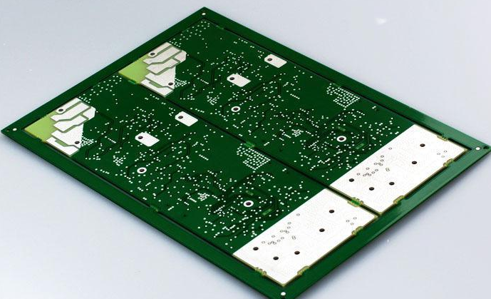
The 8 layers PCB typically uses the following three layers.
The first type of stacking is:
Layer 1: Component surface, microstrip wiring layer
Second layer: internal microstrip alignment layer, better alignment layer
Layer 3: Strata
Layer 4: Strip line layer, better line layer
Layer 5: Strip Line Line Layer
Layer 6: Power Layer
Layer 7: Internal microstrip alignment layer
Layer 8: Microstrip Wiring Layer
As can be seen from the above description, this kind of stacking method has only one power layer and one stratum, so it is not a good stacking method because of its poor electromagnetic absorption capacity and high power impedance.
The second way of stacking is:
First layer: component surface, microstrip line layer, good line layer
Layer 2: Formation, better absorption of electromagnetic waves
Layer 3: Strip Line Line Layer, Good Line Layer
Layer 4: Power Layer, which forms excellent electromagnetic absorption with the underlying strata
Layer 5: Strata
Layer 6: Strip line layers, good line layers
Layer 7: strata with large power impedance
Layer 8: Microstrip line layer, good line layer

From the above description, this method adds a reference layer, has good EMI performance, and the characteristic impedance of each signal layer can be well controlled.
The third way of stacking is:
First layer: component surface, microstrip line layer, good line layer
Layer 2: Formation, better absorption of electromagnetic waves
Layer 3: Strip Line Line Layer, Good Line Layer
Layer 4: Power Layer, which forms excellent electromagnetic absorption with the underlying strata
Layer 5: Strata
Layer 6: Strip line layers, good line layers
Layer 7: Stratum, better absorption of electromagnetic waves
Layer 8: Microstrip line layer, good line layer
The third type of stacking is the best because it uses a multilayer ground reference plane and has excellent magnetic absorption.
The following describes the stacking and impedance from a previous project.
This project has made 8 layers of plates. On the laminated side, there are three core boards (with copper on both sides, which can be seen as a two-layer board), three core boards have 6 layers, and then the upper curing sheet and the copper sheet on both sides can form 8 layers.
Route impedance design requirements:
1, highlight part L8 layer reference L7 impedance 100 Euros
2, highlight part L3 layer reference L2/L4 impedance 100 Euros
3. Highlight part L8 layer references L7 for impedance of 90 Euros
4. Highlight part L8 layer reference L7 for impedance 50 Euros
5. Highlight part L6 layer reference L5/L7 for impedance 50 Euros
6. Highlight part L3 layer reference L2/L4 for impedance 50 Euros
7. Highlight part L1 layer refers to L2 for impedance 50 Euros