What are the instructions for PCBA processing appearance inspection
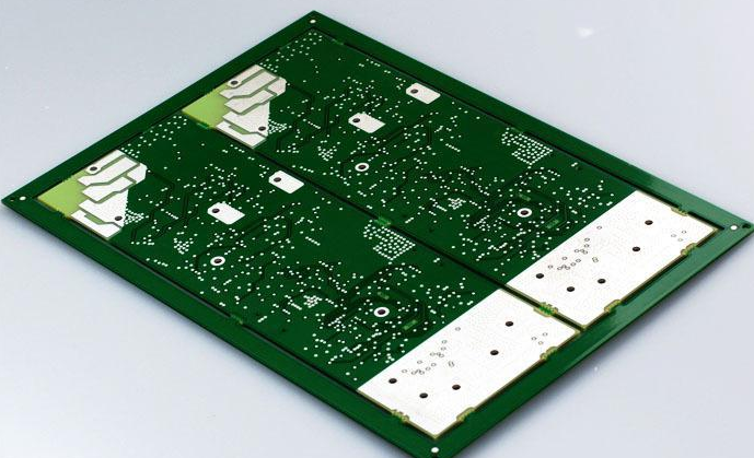
PCBA processing printed circuit boards, also known as printed circuit boards, printed circuit boards, often use the English abbreviation PCBA, which is an important electronic component, a support for electronic components, and a provider of circuit connections for electronic components. Because it is made using electronic printing technology, it is called a "printed" circuit board. Before the advent of printed circuit boards, the interconnection between electronic components relied on the direct connection of wires to form a complete circuit.
Now, the circuit breadboard only exists as an effective experimental tool, and the printed circuit board has become an absolute dominant position in the electronics industry. But most people still don't know what the PCBA processing appearance inspection instructions are? Let's learn about it with the editor of PCBA processing.
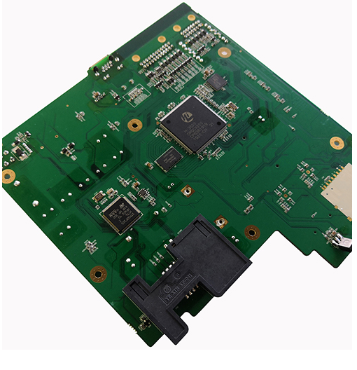
PCBA processing appearance inspection instructions

• Missing parts: The components are not mounted as required in the corresponding position on the PCBA.
• Empty soldering: 3/4 of the area of the solder joints with no or less solder on the component feet (SMD components are less than 1/2 of the width of the component).
• Lian tin: Due to abnormal operation, the two points that were originally unconnected were connected with tin.
• Wrong parts: The components mounted on the PCBA do not match those shown on the BOM
• Welding: The component pins are not well tinned, and effective welding cannot be guaranteed (including false welding)
• Cold welding: The surface of the solder joint is gray without good wetting.
• Reverse: After the component is mounted, the polarity is opposite to that specified in the document
• Tombstone: One end of the patch component is lifted away from the pad to form a tombstone
• Back: The front of the module (the silk-screened side) is facing down, but the welding is normal
• Open circuit: the component pin is disconnected or the circuit on the PCBA board is disconnected
• Tombstone: One end of the patch component is lifted away from the pad to form a tombstone
• Back: The front of the module (the silk-screened side) is facing down, but the welding is normal
• Open circuit: the component pin is disconnected or the circuit on the PCBA board is disconnected
• Lifting: The copper foil or pad of the circuit is lifted from the PCBA surface and exceeds the specification
• Multiple pieces: The file indicates the location of no components, and there are components on the corresponding PCBA board
• Tin cracking: usually after the solder joint is subjected to external force, the solder joint and the component pin are separated, which will affect the soldering effect or hidden danger. Our factory is located in China. For decades, Shenzhen has been known as the world's electronics R&D and manufacturing center. Our factory and website are approved by the Chinese government, so you can skip the middlemen and buy products on our website with confidence. Because we are a direct factory, this is the reason why 100% of our old customers continue to purchase oniPCB. You can order as little as 1 PCB from us. We will not force you to buy things you really don't need to save money.
Free DFM
Before you pay in the most timely manner, all your orders will receive free engineering document review services by our well-trained professional and technical personnel.