PCBA semi-finished product incoming inspection specification
Our factory is located in China. For decades, Shenzhen has been known as the world's electronics R&D and manufacturing center. Our factory and website are approved by the Chinese government, so you can skip the middlemen and buy products on our website with confidence. Because we are a direct factory, this is the reason why 100% of our old customers continue to purchase on iPCB.
No minimum requirements
You can order as little as 1 PCB from us. We will not force you to buy things you really don't need to save money.
Free DFM
Before you pay in the most timely manner, all your orders will receive free engineering document review services by our well-trained professional and technical personnel.
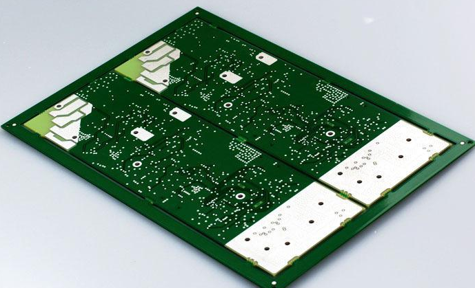
1. The appearance inspection standard of PCBA semi-finished products:
1. There is no discrepancy between the part polarity mark and the PCB polarity mark;
2. There are no parts falling off or missing soldering parts on the PCB pad;
3. There is no over-material phenomenon on PCB pads;
4. The parts on the PCB pad are consistent with the BOM material number, and there is no discrepancy;
5. There is no reverse phenomenon of parts;

6. There are no cracks or holes in the foot of the part, and no damage or deformation to the body of the part;
7. The PCB board has no obvious deformation or warping, which affects the assembly phenomenon, and no parts are severely tilted to cause poor assembly;
8. There is no part pin that does not pass through the PCB through hole, no part pin is broken, and no solder connection phenomenon with the PCB pad;
9. No obvious flux residue/foreign body phenomenon;
10. No false welding, false welding, empty welding, cold welding phenomenon.
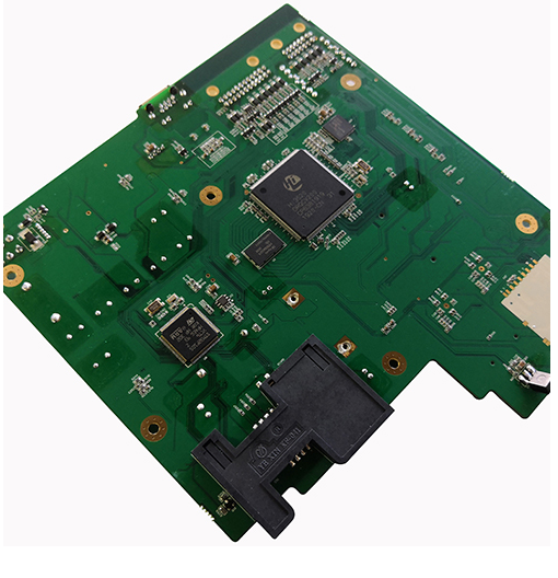
2. PCBA semi-finished product structure/dimension inspection standard:
1. Carry out size inspection according to the size requirements of the drawing/approval;
2. Inspect the circuit and parts according to the drawing/model/approval.
Three, PCBA semi-finished product functional performance test
1. Function test: According to the drawings/approval parameters, confirm whether the conduction and output meet the approval requirements.
Fourth, PCBA semi-finished product packaging/labeling standards
1. Check the packing method and quantity of the incoming materials according to the incoming material receipts/drawings/acknowledgements, and confirm that the incoming materials are clearly and completely marked;
2. There should be no short-packing, mixing, damaged packaging, dirty packaging and other undesirable phenomena. Pay attention to product innovation in terms of energy saving and emission reduction. PCB factories must learn to attach importance to Internet technology and realize the practical application of automated monitoring and intelligent management in production through the integration of overall industry knowledge.
Paying attention to the trend of environmental protection informatization and the development of various environmental protection technologies, PCB factories can start with big data to monitor the company's pollution discharge and governance results, and find and solve environmental pollution problems in a timely manner. Keep up with the production concept of the new era, continuously improve resource utilization, and realize green production. Efforts to make the PCB factory industry realize an efficient, economical and environmentally friendly production model, and actively respond to the country's environmental protection policy.