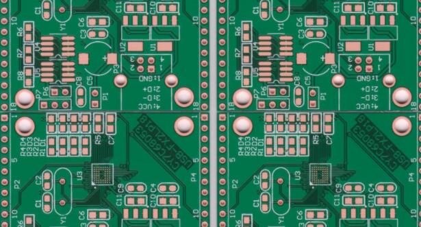
What are the PCBA processing single and double sided smt patch processes
1. Single-sided assembly:
Incoming inspection => silk screen solder paste (point patch glue) => patch => drying (curing) => reflow soldering => cleaning => inspection => repair
2. Double-sided assembly:
A: Incoming inspection => PCB's A-side silk-screen solder paste (point SMD glue) => SMD PCB's B-side silk screen solder paste (point SMD glue) => SMD => Drying => Reflow soldering ( It is best to only apply to side B => cleaning => inspection => repair).
B: Incoming inspection => PCB's A side silk screen solder paste (point patch glue) => SMD => Drying (curing) => A side reflow soldering => Cleaning => Turnover = PCB's B side point Patch glue => patch => curing => B surface wave soldering => cleaning => inspection => repair)
This process is suitable for reflow soldering on the A side of the PCB and wave soldering on the B side. In the SMD assembled on the B side of the PCB, this process should be used when there are only SOT or SOIC (28) pins or less.

3. Single-sided mixed packaging process:
Incoming inspection => PCB's A-side silkscreen solder paste (point patch glue) => SMD => drying (curing) => reflow soldering => cleaning => plug-in => wave soldering => cleaning => inspection = > Rework
4. Double-sided mixed packaging process:
A: Incoming inspection => PCB's B side point patch glue => SMD => curing => flipping => PCB's A side plug-in => wave soldering => cleaning => inspection => rework, paste first, then insert, It is suitable for the situation where there are more SMD components than separate components.
B: Incoming inspection => PCB's A side plug-in (pin bend) => flip board => PCB's B side patch glue => patch => curing => flip board => wave soldering => cleaning => Inspection => Rework, insert first, then paste, suitable for the situation where there are more separate components than SMD components.
C: Incoming inspection => PCB A side silk screen solder paste => Patch => Drying => Reflow soldering => Plug-in, pin bending => Turnover => PCB side B point patch glue => Patch => curing => flipping => wave soldering => cleaning => inspection => rework A-side mixed assembly, B-side mounting.
D: Incoming inspection => PCB's B side point patch glue => patch => curing => flip board => PCB's A side silk screen solder paste => patch => A side reflow soldering => plug-in => Wave soldering on side B => cleaning => inspection => rework for mixed mounting on side A and mounting on side B. First paste on both sides of SMD, reflow soldering, then inserting, wave soldering E: Incoming inspection => PCB's B-side silk screen solder paste (point patch glue) => SMD => drying (curing) => reflow soldering = > Flip board => PCB's A-side silk screen solder paste => SMD => Drying = Reflow soldering 1 (partial soldering can be used) => Plug-in => Wave soldering 2 (If there are few components, manual soldering can be used) => Cleaning => Inspection => Rework A-side mounting and B-side mixed mounting.
Five, double-sided assembly process
A: Incoming inspection, PCB A side silk screen solder paste (point patch glue), patch, drying (curing), A side reflow soldering, cleaning, flipping; PCB B side silk screen solder paste (point patch Glue), patch, drying, reflow soldering (preferably only for side B, cleaning, testing, and rework) This process is suitable for picking when large SMDs such as PLCC are attached to both sides of the PCB.
B: Incoming inspection, PCB A side silk screen solder paste (dot patch adhesive), patch, drying (curing), A side reflow soldering, cleaning, flipping; PCB B side dot patch adhesive, patch, Curing, B-side wave soldering, cleaning, inspection, rework) This process is suitable for reflow on the A-side of the PCBA.