Five key design points for PCBA processing circuit boards
In the past ten years, China's printed circuit board (PCB) manufacturing industry has developed rapidly, and its total output value and total output have both ranked first in the world. Due to the rapid development of electronic products, price wars have changed the structure of the supply chain. China has both industrial distribution, cost and market advantages, and has become the world's most important printed circuit board production base.
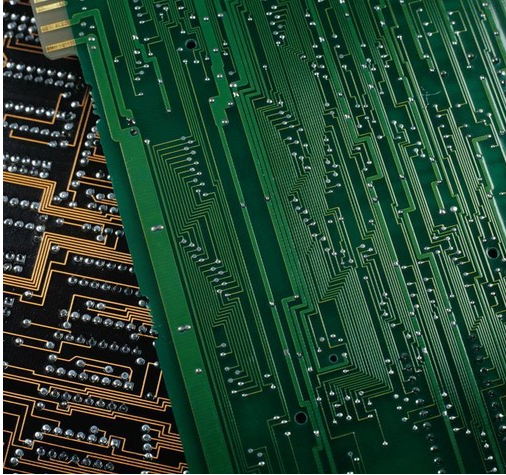
Printed circuit boards have developed from single-layer to double-sided boards, multilayer boards and flexible boards, and continue to develop in the direction of high precision, high density and high reliability. Continuously shrinking volume, reducing costs, and improving performance have enabled printed circuit boards to maintain strong vitality in the development of electronic products in the future.
The future development trend of printed circuit board manufacturing technology is to develop in the direction of high density, high precision, fine aperture, fine wire, small pitch, high reliability, multilayer, high-speed transmission, light weight, and thinness in performance.
Five key points of PCB circuit board design
There must be a reasonable direction
Such as input/output, AC/DC, strong/weak signal, high frequency/low frequency, high voltage/low voltage, etc. Their direction should be linear (or separated), and they should not blend with each other. Its purpose is to prevent mutual interference. The best trend is in a straight line, but it is generally not easy to achieve. The most unfavorable trend is a circle. Fortunately, isolation can be set to improve. For DC, small signal, low voltage PCB design requirements can be lower. So "reasonable" is relative.

2. Choose a good grounding point: the grounding point is often the most important
I don’t know how many engineers and technicians have talked about the small grounding point, which shows its importance. Under normal circumstances, a common ground is required, such as: multiple ground wires of the forward amplifier should be merged and then connected to the main ground, and so on. In reality, it is difficult to achieve this completely due to various restrictions, but we should try our best to follow it. This problem is quite flexible in practice. Everyone has their own set of solutions. It is easy to understand if they can explain it for a specific circuit board.
3. Reasonably arrange power filter/decoupling capacitors
Generally, only a number of power filter/decoupling capacitors are drawn in the schematic, but they are not pointed out where they should be connected. In fact, these capacitors are set up for switching devices (gate circuits) or other components that require filtering/decoupling. These capacitors should be placed as close as possible to these components. If they are too far away, they will have no effect. Interestingly, when the power supply filter/decoupling capacitors are arranged properly, the problem of grounding points becomes less obvious.
4. There is a requirement for the line diameter to be the appropriate size of the buried hole through hole
If possible, wide lines should never be thin; high-voltage and high-frequency lines should be round and slippery, without sharp chamfers, and corners should not be at right angles. The ground wire should be as wide as possible, and it is best to use a large area of copper, which can greatly improve the problem of grounding points. The size of the pad or via is too small, or the size of the pad and the hole size are not properly matched. The former is unfavorable for manual drilling, and the latter is unfavorable for CNC drilling. It is easy to drill the pads into a "c" shape, and to drill off the pads. The wire is too thin, and the large area of the unwiring area is not provided with copper, which is easy to cause uneven corrosion. That is, when the unwiring area is corroded, the thin wire is likely to be over corroded, or it may appear to be broken, or completely broken. Therefore, the role of setting copper is not only to increase the area of the ground wire and anti-interference.
5. Number of vias, solder joints and line density
Some problems are not easy to be found in the early stage of circuit production, and they tend to emerge in the later stage. For example, if there are too many wire holes, the slightest carelessness in the copper sinking process will bury hidden dangers. Therefore, the design should minimize the line holes. The density of parallel lines in the same direction is too large, and it is easy to join together when welding. Therefore, the line density should be determined according to the level of the welding process. The distance of the solder joints is too small, which is not conducive to manual welding, and the welding quality can only be solved by reducing the work efficiency. Otherwise, hidden dangers will remain. Therefore, the minimum distance of solder joints should be determined by comprehensive consideration of the quality and work efficiency of the welding personnel.