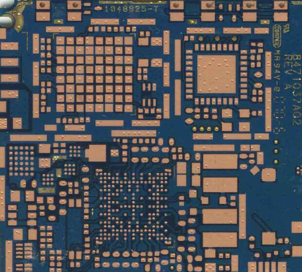
Talking about PCB etching process and its measures
First look at what is called the PCB board etching process, which uses a traditional chemical etching process to corrode unprotected areas. It's a bit like digging a trench. It's a feasible but inefficient method. The etching process is also divided into positive film process and negative film process. The positive film process uses a fixed tin protection circuit, and the negative film process uses a dry film or a wet film to protect the circuit. Using traditional etching methods to the edge of the line or pad is deformed. Every time the line increases by 0.0254mm, its edge will have a certain slope. In order to ensure sufficient spacing, the wire gap is always measured at the closest point of each pre-set wire.

In order to create a larger gap in the vacancy of the wire, it takes more time to etch an ounce of copper. This is the so-called etching coefficient. Under the premise that the manufacturer does not provide a clear list of the minimum gap per ounce of copper, understand the manufacturer's etching coefficient. It is very important to calculate the minimum capacity per ounce of copper. The etching factor also affects the manufacturer's ring hole. The traditional ring hole size is 0.0762mm imaging + 0.0762mm drilling + 0.0762 stacking, a total of 0.2286. Etching or etching coefficient is one of the four main items of the specified process level.
In order to prevent the protective layer from falling off and meet the process spacing requirements of chemical etching, traditional etching stipulates that the minimum spacing between wires should not be less than 0.127mm. Taking into account the phenomenon of internal corrosion and undercut during the etching process, the width of the wire should be increased. This value is determined by the thickness of the same layer. The thicker the copper layer, the longer it takes to etch the copper between the wires and under the protective coating. Above, there are two data that must be considered for chemical etching: the etching coefficient --- the number of etchings per ounce of copper; the minimum gap or pitch width per ounce of copper.
iPCB is happy to be your business partner. Our business goal is to become the most professional prototyping PCB manufacturer in the world. With more than ten years of experience in this field, we are committed to meeting the needs of customers from different industries in terms of quality, delivery, cost-effectiveness and any other demanding requirements. As one of the most experienced PCB manufacturers and SMT assemblers in China, we are proud to be your best business partner and good friend in all aspects of your PCB needs. We strive to make your research and development work easy and worry-free.
quality assurance
iPCB has passed ISO9001:2008, ISO14001, UL, CQC and other quality management system certifications, produces standardized and qualified PCB products, masters complex process technology, and uses professional equipment such as AOI and Flying Probe to control production and X-ray inspection machines. Finally, we will use double FQC inspection of appearance to ensure shipment under IPC II standard or IPC III standard.
Printed circuit board factory.jpg
We are not an agent
Our factory is located in China. For decades, Shenzhen has been known as the world's electronics R&D and manufacturing center. Our factory and website are approved by the Chinese government, so you can skip the middlemen and buy products on our website with confidence. Because we are a direct factory, this is the reason why 100% of our old customers continue to purchase on iPCB.
No minimum requirements
You can order as little as 1 PCB from us. We will not force you to buy things you really don't need to save money.
Free DFM
Before you pay in the most timely manner, all your orders will receive free engineering document review services by our well-trained professional and technical personnel.