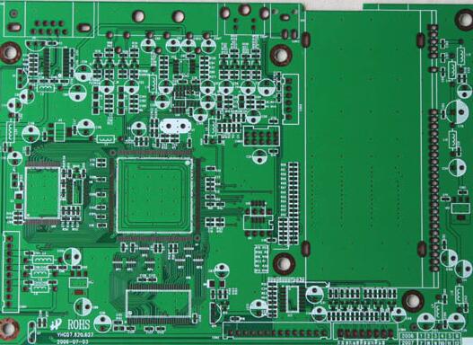
Application specification of through-hole design in high-speed PCB board
As we all know, in high-speed PCB design, seemingly simple through-hole PCBs often have a great negative impact on circuit design. Therefore, in the design, we should try our best to do the following:
1. Considering both cost and signal quality, choose a reasonable through hole size. For example, for a 6-10 layer memory module PCB design, it is best to choose a 10/20mil (drilled/soldered pad) through-hole PCB. For some small-sized high-density boards, you can also try to use 8/18mil through-hole PCBs under current technical conditions. It is difficult to use smaller-sized through-holes. For through-hole PCBs for power or ground wires, a larger size can be considered to reduce impedance.
2. Use a thinner PCB board, which helps to reduce the two parasitic parameters through holes.
3. Try not to change the signal routing layer on the PCB board, that is, try not to use unnecessary holes.

4. The power and ground pins should be closest to the hole, and the shorter the hole and the pin, the better, because they will increase the inductance. At the same time, the power and ground leads should be as thick as possible to reduce impedance.
5. Set a ground hole near the hole in the signal layer to make the signal provide the nearest loop. In addition, remember that the process needs to be flexible. The through-hole PCB model has pads on each layer. Of course, we can also reduce or even remove some layer pads. Especially when the density of through holes is very high, it may cause grooves separating circuits to appear in the copper layer. At this time, in addition to moving the position of the via, you can also consider reducing the size of the via pad in the copper layer.
Our factory is located in China. For decades, Shenzhen has been known as the world's electronics R&D and manufacturing center. Our factory and website are approved by the Chinese government, so you can skip the middlemen and buy products on our website with confidence. Because we are a direct factory, this is the reason why 100% of our old customers continue to purchase on iPCB.
No minimum requirements
You can order as little as 1 PCB from us. We will not force you to buy things you really don't need to save money.
Free DFM
Before you pay in the most timely manner, all your orders will receive free engineering document review services by our well-trained professional and technical personnel.
On-time delivery
Over the years, we are proud to maintain a 99% on-time delivery rate. We work in three shifts to ensure that your PCB can appear on your desk as planned and as early as possible. You can choose DHL and other courier services to balance speed and budget. We only use services from reliable and reputable companies.