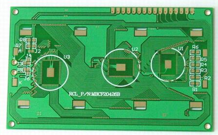
In the circuit board industry, especially in the engineering department, we often hear terms such as via and pad. Many friends do not understand what it means. Let’s talk about the meaning of via and pad in detail. In production What are the differences in processing methods.

Circuit board via introduction
Via is called a via, which is divided into through holes, blind holes and buried holes. It is mainly used for the connection of wires in different layers of the same network, and is generally not used as a soldering component. in:
1. Blind holes are used to connect the surface circuit and the inner circuit(only available in multi-layer boards, that is, only one head of the hole can be seen, and the other head does not penetrate the board).
2. Buried vias are the connection between the inner layer and the inner layer (only available in multi-layer boards, the buried holes cannot be seen on the outside)
3. Through holes are holes that penetrate the surface and bottom layers and are used for internal interconnection or as installation positioning holes for components.
The only used for the connection of the circuit is the via hole, which is small in size. The holes used to install soldering components are generally larger than the via holes. Vias consist of drilled holes and pads.
The simplest understanding is: the pad is a larger hole for soldering components. The via is very small, just a hole that connects lines of different layers.
In a professional and simple way:
1, a via is a hole that connects the middle layer and the layer in a double or multilayer; it is characterized by electrical conductivity and is not used for welding;
2. Drilling is a mechanical hole on the PCB board, which is used for assembly. It does not necessarily have electrical properties and cannot be soldered;
3. The pad is used to fix the perforated or gold-plated surface of the electronic device (surface pad SMD PAD), which is characterized by electrical conductivity and can be soldered.
Circuit board pad introduction
Pad is called a pad, which is divided into pin pads and surface mount pads; pin pads have solder holes, which are mainly used for soldering pin components; while surface mount pads have no solder holes and are mainly used for soldering surface mount components.
Via mainly plays the role of electrical connection, the aperture of via is generally small, usually as long as the board processing technology can do it, it is enough, and the surface of the via can be coated with solder mask ink or not; while the pad is not only used for electrical The role of the connection, but also the role of mechanical fixing, the aperture of the pad (of course the pin pad) must be large enough to pass through the pin of the component, otherwise it will cause production problems;
In addition, the surface of the pad must not have solder mask ink, because this will affect the soldering, and usually flux is applied to the surface of the pad when making the board; there is also the diameter of the pad’s aperture (when it refers to the pin pad) and The apertures must also meet certain standards, otherwise it will not only affect the welding, but also cause the installation to be unstable.
Different treatment methods
1. As much as VIA’s holes are indicated in the design, the drilling is as much as possible. Then it has to go through process steps such as copper sinking, and the final actual aperture will be about 0.1mm smaller than the designed aperture. For example, if the via hole is set to 0.5mm, the actual aperture after completion is only 0.4mm.
2. The hole diameter of the PAD will increase by 0.15mm when drilling. After the copper sinking process, the hole diameter is slightly larger than the designed hole diameter, about 0.05mm. For example, if the designed hole diameter is 0.5mm, the drilling hole will be 0.65mm, and the finished hole diameter will be 0.55mm.
3, VIA will be covered with green oil in some default PCB processes, it may be blocked by green oil and cannot be soldered. Test points can't be done either.
4. The minimum width of VIA's welding ring is 0.15mm (under the general process) to ensure reliable copper plating.
5. The minimum width of the solder ring of the PAD is 0.20mm (under the general process) to ensure the adhesion of the pad.