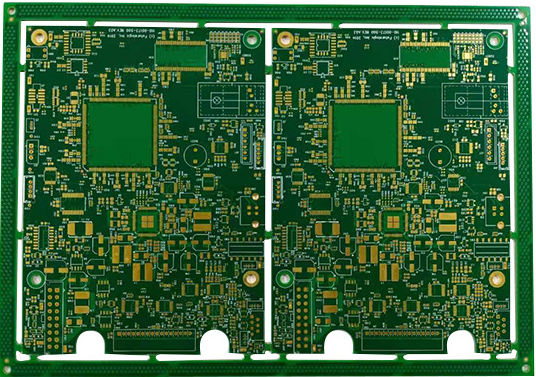
A brief talk on the trend of PCB substrates for circuit boards
1. Continuous innovation of FR-4 board
In short, PCB circuit board substrates mainly include three major raw materials: copper foil, resin, and reinforcing materials. However, if you further study the current substrate and examine its changes over the years, you will find that the complexity of the substrate content is really unimaginable. As circuit board manufacturers have increasingly stringent requirements for the quality of substrates in the lead-free era, the performance and specifications of resins and substrates will undoubtedly become more complex. The challenge faced by substrate suppliers is to find the best balance between the various needs of customers in order to obtain the most economical production benefits, and provide their product data to the overall supply chain as a reference.
2. Industry trends leading the specifications of substrates
A number of ongoing industrial trends will promote the market application and adoption of reformulated panels. These trends include the design trend of multi-layer panels, environmental protection regulations, and electrical requirements, which are described below:
2.1. Design trend of multi-wide board
One of the current PCB design trends is to increase the wiring density. There are three ways to achieve this goal: The first is to reduce its line width and line spacing, so that more and more dense wiring can be accommodated in a unit area; the second is to increase the circuit board layer. Number; the last is to reduce the aperture and the size of the solder pad.

However, when there are more lines per unit area, its operating temperature is bound to rise. Furthermore, as the number of layers of circuit boards is continuously increased, the finished boards will inevitably become thicker at the same time. Otherwise, it can only be laminated with a thinner dielectric layer to maintain the original thickness. The thicker the PCB, the more the thermal stress of the through-hole wall caused by the heat accumulation will increase, which will increase the thermal expansion effect in the Z direction. When a thinner dielectric layer is selected, it means that a substrate and film with a higher glue content must be used; but a higher glue content will cause the thermal expansion and stress in the Z direction of the through hole to increase. In addition, reducing the aperture of the through hole will inevitably increase the aspect ratio; therefore, in order to ensure the reliability of the plated through hole, the substrate used must have lower thermal expansion and better thermal stability so as not to fall short.
In addition to the above factors, when the density of the assembly components of the circuit board increases, the layout of the via holes will also be arranged more closely. However, this action will make the leakage of the glass bundle more tense, and even bridge the substrate glass fiber between the hole walls, which will lead to a short circuit. This kind of anodic filiform leakage phenomenon (CAF) is one of the themes of the current lead-free era for sheet materials. Of course, the new generation of substrates must have better anti-CAF ability to prevent frequent occurrences in lead-free soldering. .
2.2. Environmental protection laws and regulations
Among many regulations, RoHS restricts the lead content during soldering. Tin-lead solder has been used in assembly plants for many years. The melting point of its alloy is 183°C, and the temperature of the fusion soldering process is generally about 220°C.
Lead-free mainstream solder tin-silver-copper alloys (such as SAC305 has a melting point of about 217°C, and usually peak temperature during fusion soldering will be as high as 245°C. The increase in soldering temperature means that the base material must have better thermal stability before it can be tolerated. Thermal shock caused by multiple fusion welding.
The RoHS directive also bans certain halogen-containing flame retardants, including PBB and PBDE. However, TBBA, the most commonly used flame retardant in PCB substrates, is actually not on the RoHS blacklist. Nevertheless, due to the improper ashing reaction of TBBA-containing plates when the temperature is raised, some brand manufacturers of the whole machine still consider changing to halogen-free materials.
2.3. Electrical requirements
PCB circuit boards have electrical requirements, high-speed, broadband, and radio frequency applications, forcing the board to have better electrical performance, that is, the dielectric constant Dk and the dissipation factor Df must not only be suppressed, but also must be full board. The performance is stable in the medium and should also be well controlled. Those who meet these electrical requirements also have to be inferior in thermal stability. Only in this way, their market demand and market share can increase day by day.