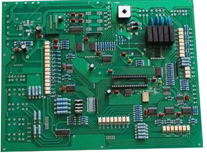
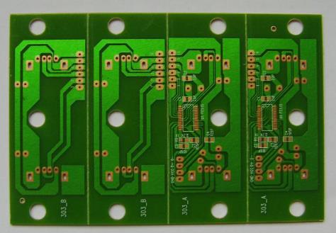
In maintaining signal integrity, differential pairs must be correctly wired in high-speed PCB digital circuits. Follow these differential pair routing guidelines and leave your EMI issues behind.
Differential routing tips and tricks
Tracking length matching: When routing differential pairs, tracking length matching should be the primary task. Don't let one signal go all the way through the printed circuit board, while the other signal must go to the next door. When the length of the differential pair traces does not match, the timing difference will cause destructive interference and reduce signal integrity. Similar to my date height preference may be different from yours, different circuits have different trace length mismatch tolerances. Before starting the design, make sure your differential pair is clearly visible and check their mismatch tolerance.
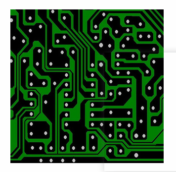
Parallel routing: Whenever routing differential pairs, try to keep their traces parallel. Parallel routing of differential pairs helps to counteract any radiated EMI and helps track length matching.

Electrical clearance and creepage distance: Like current and ex-girlfriends, a single differential pair should always be kept as far away as possible. When multiple differential pairs are closely routed, they will always interact in a negative way. In the case of extremely long distances, the advantage is maintained and EMI is minimized.
Differential pairs also need to be far away from components that are susceptible to EMI. Measure this distance in distance and creepage distance. There are many different ways to meet the clearance and creepage distance requirements of the circuit.
No sharp turns: It is best to route the differential pair directly without turning at all. However, your PCB layout may need to be turned. Some women like smooth men, but the difference pairs always like smooth curves. Sharp edges at corners will radiate more EMI than smooth curves. Any change in the direction of the differential pair should not deviate more than 45 degrees. This is important at both the internal and external edges, as both can radiate EMI.
Vias: Just like having many girlfriends is not a good idea, using a lot of filters is not a good idea. The geometry ensures at least a small amount of signal degradation. When used too frequently, vias can significantly reduce signal integrity and cause destructive reflections in the differential pair.
If you end up using vias on the printed circuit board, make sure to shorten the short wire length or reverse drill the stub. The through-hole stub will act as an open transmission line, which means a lot of signal reflection. Depending on the length of the stub, the signal can even be reflected 180 degrees back to the differential pair and cancel the useful signal. The best way to reduce the negative effects of stubs is to minimize the length of the stubs. By using blind holes or buried holes, or through short column back drilling, the short column length can be minimized. All of these options increase manufacturing costs, so if the budget is tight, you can simply establish a pathway connection on the remote board. In an 8-layer circuit board, the unused stubs for the 1-7 connection are shorter than the 1-2 connection.
It is also important to match the amount of any signal delay caused by the via. This can be done by using the same number of vias in both legs of the differential pair or by adding some serpentine routing on the legs without vias. No one likes to be the third round of dating, so make sure everything matches evenly.
How to get your computer done
In order to optimize brain power, let your computer do some work. Your PCB design software should be able to automatically check some of these rules, such as electrical clearance. More advanced software can also help you implement the actual routing of differential pairs. AltiumDesigner® may not have a solution for your love life, but it does have the function of helping users perform differential pair routing.
If there is a problem with the differential pair wiring on the PCB, then your board may not be so lucky. Be sure to follow the above guidelines to maintain the signal integrity of high-speed PCB designs.