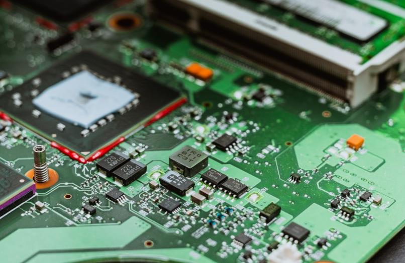
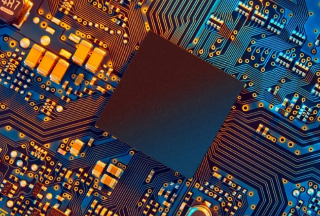
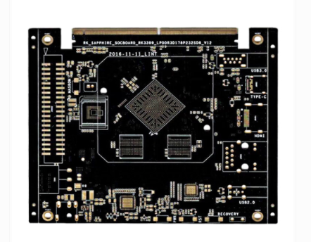
High-frequency circuit board refers to the special circuit board with high electromagnetic frequency, which is used in the fields of high frequency (frequency greater than 300MHZ or wavelength less than 1 meter) and microwave (frequency greater than 3GHz or wavelength less than 0.1 meter). It is a circuit board produced on the microwave substrate copper-clad board using the common rigid circuit board manufacturing process or using special processing methods.
The substrate material of high frequency circuit board needs to have excellent electrical performance and good chemical stability. The loss on the substrate with the increase of power signal frequency is very small, so the importance of high frequency board is highlighted.
High-frequency circuit board with induction heating technology has been widely used in communication industry, network technology and high-speed information processing system, meeting the use requirements of many high-precision parameter instruments. Reliable high-frequency circuit board has provided great help in actual production. So, what are the advantages of such a powerful high-frequency circuit board?

1. High efficiency of high frequency circuit board
High-frequency circuit boards with low dielectric constant will also have low loss, and the advanced induction heating technology can meet the demand of target heating with high efficiency. Of course, while paying attention to efficiency, it also has the characteristics of environmental protection, which is very suitable for the development direction of today's society.
2. High speed of high frequency circuit board
The transmission speed of the circuit is inversely proportional to the square root of the dielectric constant, which means that the smaller the dielectric constant, the faster the transmission speed. This is the advantage of high frequency circuit board. It uses special materials, which not only ensures the low dielectric constant, but also maintains the stability of operation, which is very important for signal transmission.
3. High frequency circuit board is adjustable
High-frequency circuit boards, which are widely used in various industries for the heating treatment of precision metal materials, can not only realize the heating of parts in different depths, but also focus on the heating according to local characteristics. Whether it is surface or deep, centralized or decentralized heating, it can be easily completed.
4. High frequency circuit board has strong resistance
The dielectric constant and medium of high frequency circuit boards have certain requirements on the environment, especially the wet weather will seriously affect the use of circuit boards. High-frequency circuit boards made of materials with extremely low water absorption can challenge such environment, and also have the advantages of resistance to chemical corrosion, moisture resistance, high temperature resistance and great peeling strength, which make high-frequency circuit boards play a powerful role.
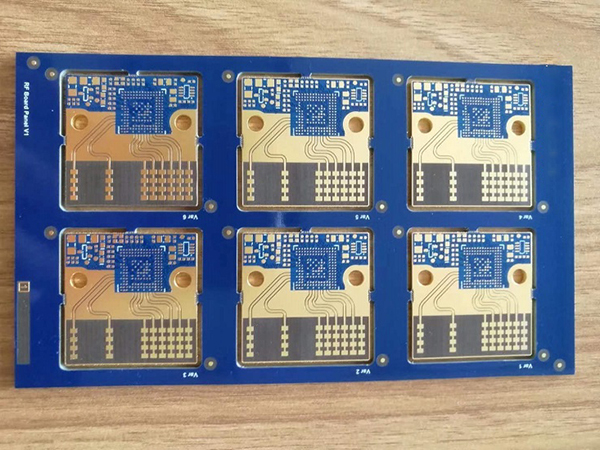
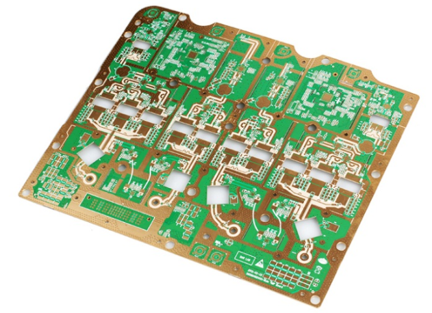
Classification of high-frequency PCB materials
1. Thermosetting materials filled with final ceramics
The processing method of thermosetting materials filled with end ceramics is similar to that of epoxy resin/glass woven fabric (FR4), but the plate is brittle and easy to break, and the service life of drill tip and gongs will be reduced by 20% when drilling and gongs.
2. PTFE (polytetrafluoroethylene) material
Processing method of PTFE (polytetrafluoroethylene) material
Material opening: protective film must be reserved to prevent scratching and indentation
Drilling: use a new drill nozzle (standard 130), one piece at a time is the best, and the pressure of the presser foot is 40psi. The aluminum sheet is the cover plate, and then use 1mm melamine backing plate to tighten the PTFE plate. After drilling, use the air gun to blow out the dust in the hole. Pay attention to the need to use the most stable drilling rig, drilling parameters (basically, the smaller the hole, the faster the drilling speed, the smaller the Chip load, the smaller the return speed)
Treatment of VIA hole: plasma treatment or sodium naphthalene activation treatment is conducive to hole metallization
PTH copper deposition: after micro-etching (the micro-etching rate is controlled by 20 microinches), the plate is fed from the cylinder at PTH. If necessary, we can pass the second PTH, and only need to start from the estimated PTH? The cylinder starts to enter the board.
Solder: use acid plate washing for soldering resistance pretreatment, do not use mechanical grinding plate, bake the plate after pretreatment (90 ℃, 30min), brush green oil for curing, and bake the plate in three sections: one section of 80 ℃, 100 ℃, 150 ℃, and 30min each (if there is oil spilling on the substrate surface, rework can be done: wash off the green oil and reactivate it)
CNC for high frequency circuit boards: lay white paper on the gongs of the high-frequency circuit board, and clamp it up and down with a FR-4 PCB or phenolic base plate with a thickness of 1.0MM etched to remove copper